

|Im Zeitalter der Multi-Gigabit-Datenübertragung, Eine Impedanzabweichung im Mikrometerbereich auf einer Leiterplatte kann die Leistung von Server-Arrays im Wert von mehreren Millionen beeinträchtigen.
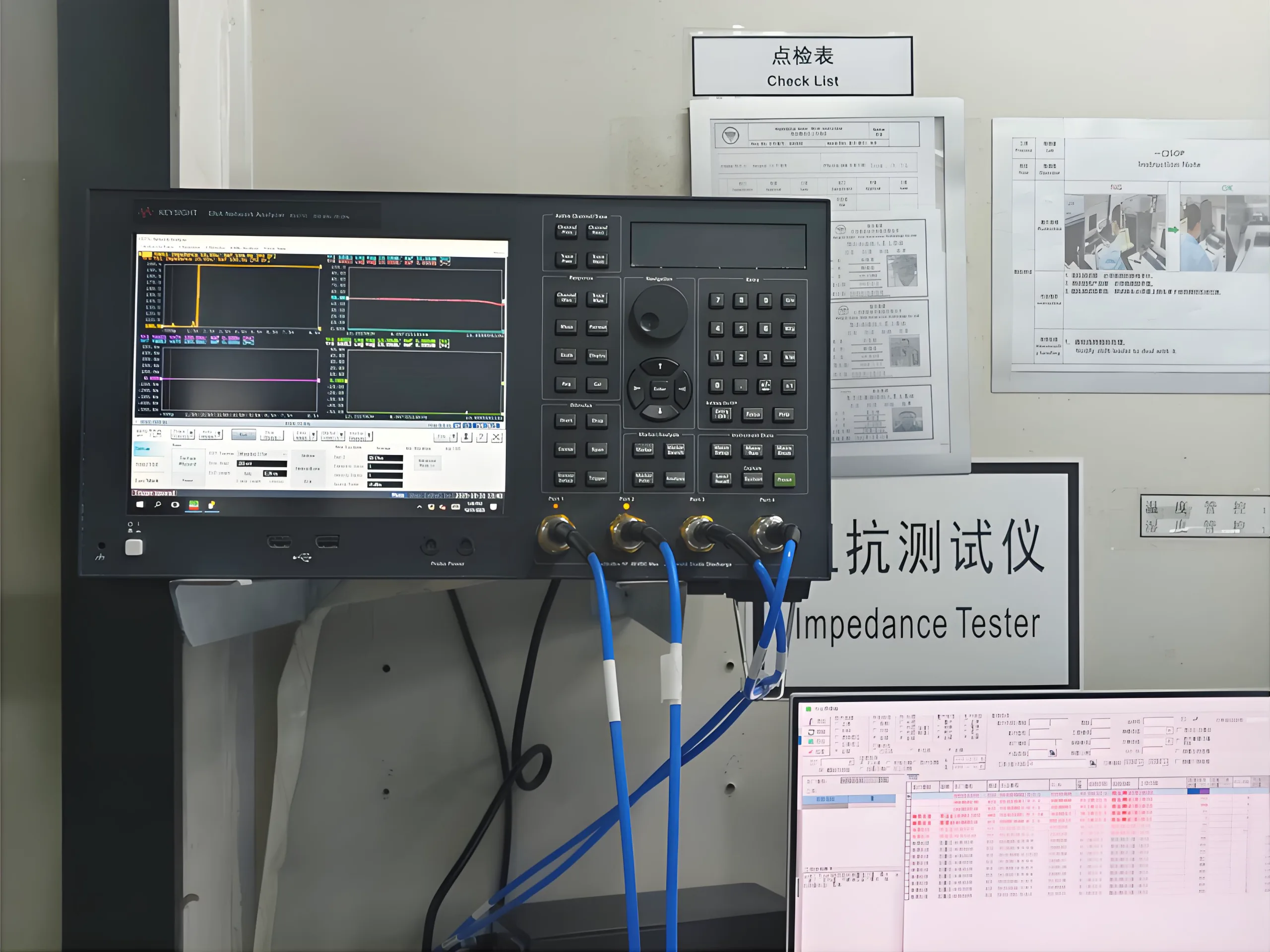
In der Einrichtung von UGPCB, Ingenieure überwachen die Impedanzdaten für Hochgeschwindigkeits-Server-Motherboards in Echtzeit. Die Kurven auf dem Bildschirm bleiben stabil Grünpassband von 100 Ω ±2 % - Die hohen Anforderungen des PCIe 5.0 Standard für Differenzimpedanz. Möglich wird dies durch unsere jüngste Investition in Spitzentechnologie Leiterplatte testen und Qualitätskontrolle Technologie.
Die Branchenherausforderung: Die Präzisionskrise im Zeitalter der Hochgeschwindigkeitssignale
Das explosive Wachstum von KI-Computing und 5G-Kommunikation hat zu einer exponentiellen Nachfrage nach schnelleren Datenraten geführt. Standards wie PCIe haben sich weiterentwickelt PCIE 5.0/6.0, mit Signalfrequenzen größer 32 GT/s und auf dem Weg dorthin 64 GT/s.
Höhere Frequenzen führen zu einem exponentiellen Anstieg der Einfügungsdämpfung, während Impedanzdiskontinuitäten in PCB-Spuren Signalreflexion und Jitter verursachen. Diese Probleme stellen die kritischsten Herausforderungen bei der Signalintegrität dar Hochgeschwindigkeits-PCB-Design und Fertigung.
Ein modernes Smartphone-Motherboard darf zumindest enthalten 12 Schichten komplexer Streckenführung. Der unaufhaltsame Trend zur Miniaturisierung erfordert schmalere Leiterbahnbreiten und engere Abstände, die Anforderungen an drängen Impedanzkontrolle in der Leiterplattenfertigung auf ein noch nie dagewesenes Niveau.
Die technische Lösung: Das Keysight-Impedanztestsystem von UGPCB
Um diese Herausforderungen anzugehen, UGPCB hat das integriert Keysight 4-Kanal 20G Impedanztestsystem, eine hochpräzise Plattform basierend auf Vector Network Analyzer (VNA) Technologie.
Die Kernhebel des Systems Die leistungsstarke Netzwerkanalysatortechnologie von Keysight, mit 4 unabhängige Testkanäle mit einem Frequenzbereich von 10 MHz zu 20 GHz. Dieses breite Band ermöglicht eine umfassende Bewertung von Hochgeschwindigkeitsverbindungen, von einfachen digitalen Schaltkreisen bis hin zu Millimeterwellenanwendungen.
Systemvorteile: Ein Dreiklang der Präzision, Effizienz, und Stabilität
-
Unübertroffene Präzision: Das System liefert eine Grundimpedanz-Messgenauigkeit von ±0,08 % (typisch ±0,045 %), mit einem Impedanzbereich von 25 mΩ zu 40 Mω. Dieses Niveau von PCB-Impedanzprüfung Präzision erkennt kleinste Abweichungen, was entscheidend ist für fortschrittliche PCBA-Fertigung.
-
Überlegene Effizienz: Es unterstützt Mehrkanal-Paralleltests, Verbesserung des Durchsatzes um bis zu 300% im Vergleich zu Einkanalgeräten. Automatisierte Testplanung ermöglicht 24/7 Batch-Testfähigkeit, Straffung der PCB-Prototyp und Montage Validierungsprozess.
-
Außergewöhnliche Stabilität: Mit Temperaturkompensationstechnologie und optische Systeme aus Materialien mit geringer Ausdehnung, Das System minimiert die Auswirkungen von Umgebungsschwankungen auf die Messergebnisse, Gewährleistung konsistenter und zuverlässiger Daten Qualitätssicherung von Leiterplatten.
Anwendung & Wert: Full-Cycle-Qualität vom Prototyp bis zur Produktion
Dieses fortschrittliche System bietet Mehrwert für das gesamte Leistungsspektrum von UGPCB, Stärkung unserer Führungsrolle in professionelle PCB und PCBA-Herstellung Dienstleistungen.
-
In R&D und Prototyping: Ingenieure können schnell validieren, wie sich unterschiedliche Aufbauten und Materialien auf die Impedanz auswirken, Verkürzung der Design-Test-Zyklen von Wochen auf Tage. Dies beschleunigt die Entwicklung von Hochfrequenz-Leiterplatten, RF -PCBs, Und HDI-Leiterplatten.
-
In der Massenproduktions-Qualitätskontrolle: Integriert in intelligente Produktionslinien, Das System führt Stichproben oder vollständige Inspektionen durch, Generieren von SPC-Diagrammen in Echtzeit. Dies ermöglicht proaktive Prozessanpassungen, Vermeidung von Chargenproblemen und Sicherstellung einer gleichbleibenden Qualität Großserienfertigung von Leiterplatten.
-
Für High-End-Anwendungen: Für kritische Anwendungen wie KI-Server-PCBs, 5G-Basisstation Leiterplatten, und Hochgeschwindigkeitsschalter, UGPCB bietet detaillierte Informationen Impedanzkonsistenzberichte. Diese Datentransparenz schafft Vertrauen bei den suchenden Kunden zuverlässige Leiterplattenlieferanten Und schlüsselfertige PCBA-Lösungen.
Die Wissenschaft hinter der Messung
Die Leistung des Systems basiert auf soliden wissenschaftlichen Prinzipien. Es beschäftigt Zeitdomäne Reflektometrie (Tdr), Das funktioniert wie ein Radar, indem es ein Signal über eine Spur sendet und Reflexionen analysiert, um Impedanzänderungen und Fehler zu lokalisieren.
Die charakteristische Impedanz (Z₀) einer Spur wird in erster Linie durch ihre Geometrie bestimmt und bei hohen Frequenzen durch die Formel angenähert:
Z₀ ≈ √(L/c)
(Dabei ist L die Induktivität pro Längeneinheit und C die Kapazität pro Längeneinheit). Dies verdeutlicht, warum die Kontrolle physikalischer Dimensionen von größter Bedeutung ist Herstellung von Leiterplatten mit kontrollierter Impedanz.
Das System nutzt auch die Delta-L-Methode, Ein fortschrittlicher Algorithmus, der Fixture-Effekte aufhebt und Mehrfachreflexionen entfernt, Bereitstellung überragender Genauigkeit für Hochgeschwindigkeits- und Hochfrequenz-PCB-Tests.
Greifbare Kundenvorteile
Die Investition in diese Fähigkeit führt zu direkten Kundenvorteilen:
-
Reduziertes Risiko: Die frühzeitige Erkennung von Impedanzabweichungen verhindert kostspielige Feldausfälle und Rückrufe.
-
Verbesserte Leistung: Eine präzise Impedanzsteuerung ermöglicht höhere Datenraten und niedrigere Bitfehlerraten, was entscheidend ist für Hochgeschwindigkeits-Digital-PCBA Und Leiterplatten für Kommunikationsgeräte.
-
Schnellere Time-to-Market: Zuverlässige Testdaten reduzieren die Designunsicherheit, Verkürzung der Validierungszeit für Hochgeschwindigkeitsschnittstellen um 40-60%.
Dieses UGPCB, Unser Engagement ist nicht nur an den Wänden unserer Einrichtung, sondern in jedem Board, das wir versenden, eingraviert: “Single-Ended Impedance 50Ω ±5%, Differenzimpedanz 100 Ω ±8 % — 30% superior to typical industry standards.” Dies ist nicht nur eine Spezifikation; Es ist unser Versprechen, die Signalintegrität im digitalen Hochgeschwindigkeitszeitalter zu schützen. Indem Sie sich für UGPCB entscheiden Leiterplattenfertigung und PCBA-Montage Bedürfnisse, Sie arbeiten mit einem Hersteller zusammen, der in der Lage ist, die Präzision zu liefern, die Ihre anspruchsvollsten Designs erfordern.