
En la industria de fabricación electrónica en rápida evolución, SMT defectos de desecho (comúnmente conocido como el efecto de Manhattan o defectos de lápida) sigue siendo un cuello de botella crítico que limita las mejoras en PCB y tarjeta de circuito impreso rendimiento de primer paso. A medida que los avances impulsados por la IA impulsan actualizaciones integrales en la tecnología de PCB, innovaciones en materiales, procesos, y las arquitecturas están marcando el comienzo de un nuevo ciclo industrial. La adopción generalizada de componentes de chips en miniatura., como 0402 (01005) paquetes, ha llevado a un resurgimiento del fenómeno de Manhattan con mayores tasas de ocurrencia, Emergiendo como un desafío inevitable en la fabricación de alta gama.. Este artículo proporciona un análisis en profundidad de las causas del destierro basado en criterios internacionales. Normas IPC y modelos mecánicos, al mismo tiempo que ofrece una estrategia de prevención de rango completo que abarca el diseño, materiales, y optimización de procesos.
El fenómeno de Manhattan: El asesino invisible en soldadura SMT
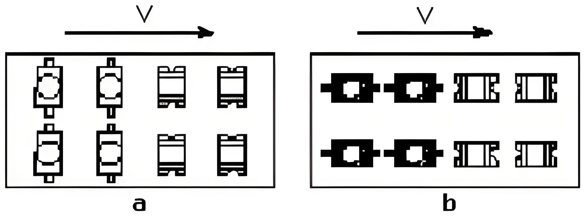
El fenómeno Manhattan es un defecto común en la soldadura por reflujo SMT, donde un extremo de un componente del chip se levanta de la almohadilla, girando verticalmente en un ángulo (normalmente entre 30° y 90°), parecido a un rascacielos o una lápida, de ahí su nombre. Este defecto no sólo compromete la conectividad eléctrica sino que también puede provocar cortocircuitos., juntas frias, y otras cuestiones, Disminución grave de la fiabilidad del producto..
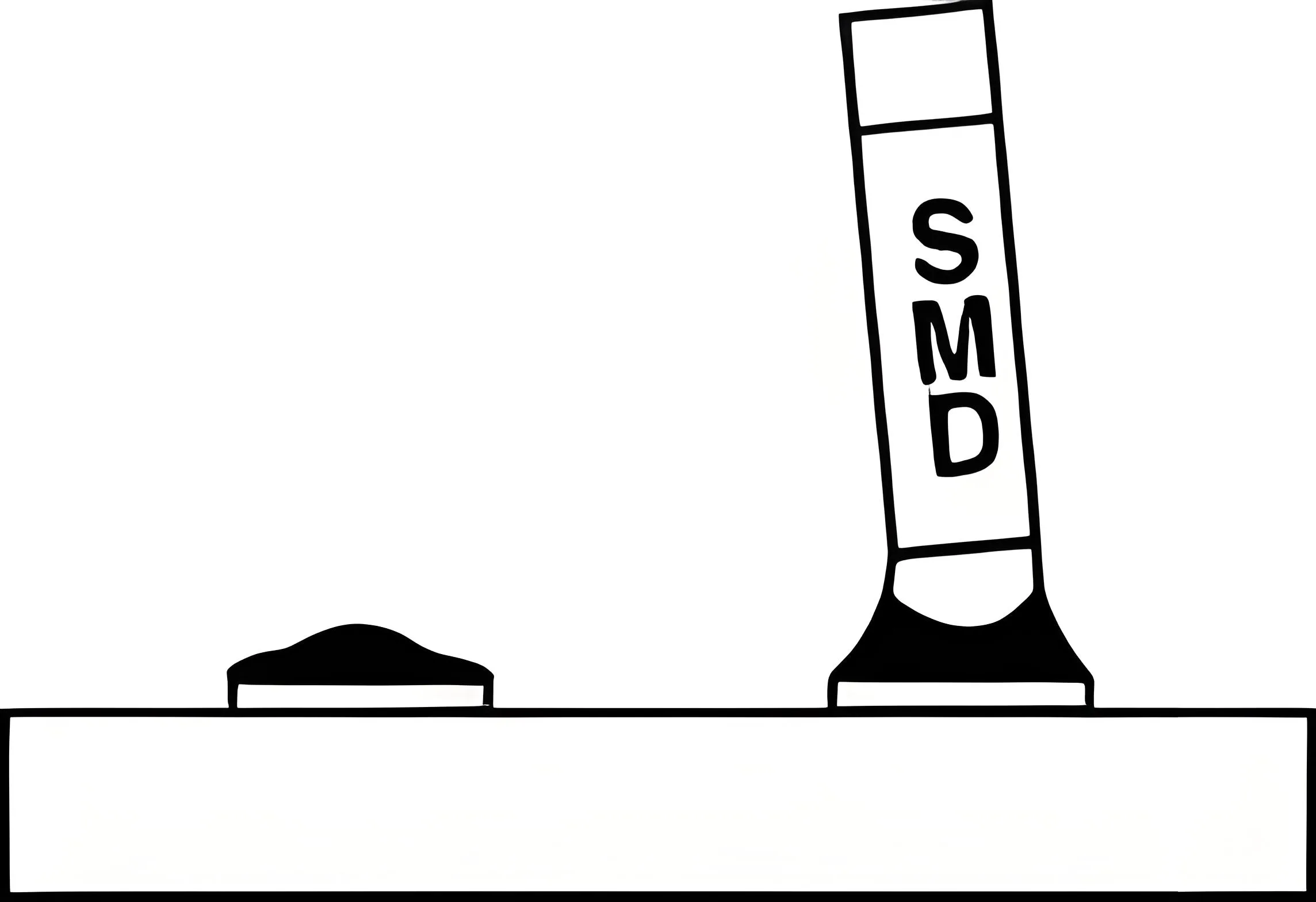
El problema central surge de un desequilibrio de par causado por fuerzas desiguales en los extremos de los componentes.. Cuando la soldadura en pasta en un extremo se funde primero y genera fuerzas de humectación, mientras que el extremo opuesto permanece sin derretir, el diferencial de tensión superficial tira del componente hacia arriba, formando una lápida. Según modelos mecánicos., El desecho ocurre cuando el factor de equilibrio Eb excede 1.
Mecanismo mecánico y parámetros clave del fenómeno de Manhattan
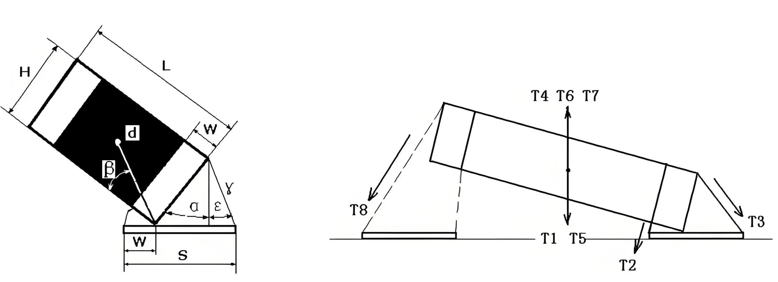
Análisis del modelo de fuerza
Las fuerzas que actúan sobre un componente durante la soldadura por reflujo son complejas e incluyen principalmente los siguientes momentos:
-
Momentos de resistencia:
-
T1 = Mgdcos(a+b) (gravedad del componente)
-
T2 = γωcos(a/2) (tensión superficial de la soldadura fundida en la parte inferior del componente)
-
T5 = Adcos(a+b) (fuerza adhesiva de la pasta de soldadura)
-
-
Momentos de conducción:
-
T3 = γHsen(a+d) (tensión superficial en el filete final del componente)
-
T6 = Mvdcos(a+b) (fuerza inducida por la vibración del transportador)
-
T7 = Lhρgdcos(a+b) (Máxima flotabilidad a partir de la generación de gas en pasta de soldadura.)
-
Factor de equilibrio Eb = (T3 + T6 + T7) / (T1 + T2 + T5)
Cuando Mib > 1, Los momentos de conducción superan los momentos de resistencia., provocando inevitablemente el efecto Manhattan.
Papel crítico de la tensión superficial
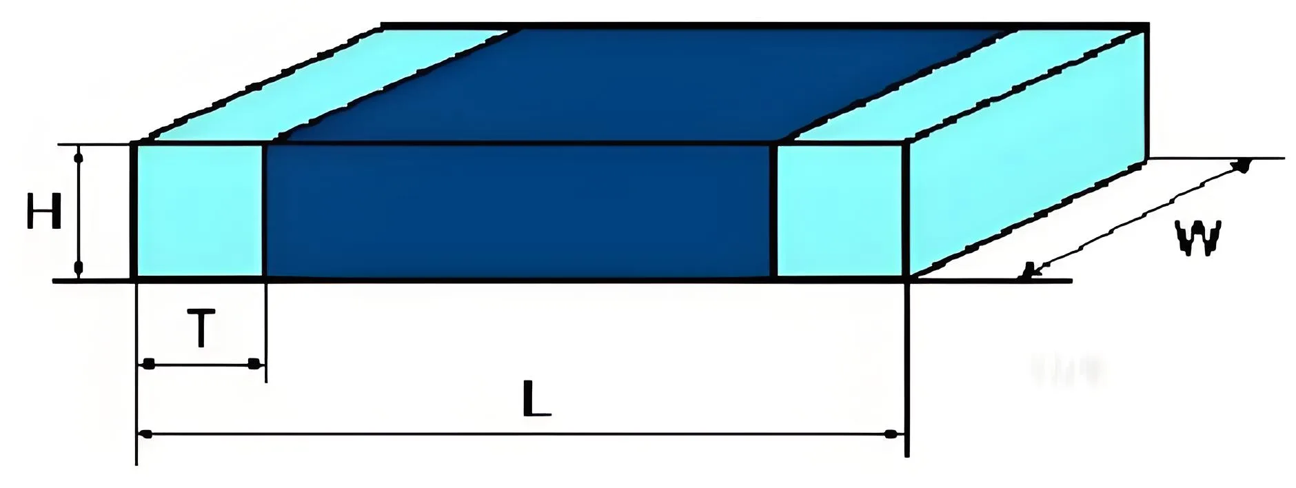
La soldadura en pasta fundida minimiza el área de superficie según el principio de minimización de energía.. Su tensión superficial se define como σ = (Fs – Fv) · n1, donde Fs es la energía libre superficial, Fv es energía libre de volumen, y n1 es el número de moléculas por unidad de área.
De la ecuación de Laplace, la presión adicional en la superficie del líquido es: Padd = 2σH, donde H = ½(1/R1 + 1/R2). Las diferencias en la curvatura de la soldadura fundida en los extremos de los componentes crean una presión adicional desigual, lo que lleva a una tensión superficial no uniforme e inicia el desmoronamiento.
Análisis de 16 Factores clave que influyen en el fenómeno de Manhattan
Diseño de PCB y factores de materiales
-
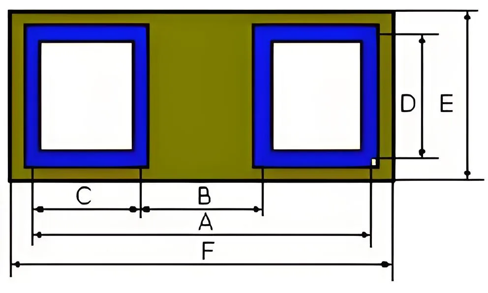
Diseño de almohadilla asimétrica: El incumplimiento de los estándares IPC-7351/IPC-SM-782 da como resultado una capacidad térmica desigual. Las dimensiones recomendadas de las almohadillas deben cumplir estrictamente con los estándares.; p.ej., para 0402 componentes, longitud de la almohadilla A = 1,50 mm, ancho B = 0,50 mm.
-
Falta de coincidencia entre los componentes y el espaciado de las almohadillas de PCB: Provoca fuerzas de humectación desequilibradas..
-
Variación de la capacidad térmica en las almohadillas: Las almohadillas más grandes tienen mayor capacidad térmica, calentar más lento, y retrasar la fusión de la soldadura.
-
Sustrato de PCB Conductividad térmica: La incidencia es mayor con sustratos epoxi de papel. (≥8%), seguido de epoxi de vidrio (≈5%), y el más bajo con cerámica de alúmina (≤2%).
-
Volumen asimétrico de soldadura en pasta: Los errores de impresión o el espesor inconsistente provocan diferencias en la capacidad térmica.
-
Contaminación u oxidación de la capa de níquel ENIG: Da como resultado una humectabilidad deficiente y un tiempo de humectación prolongado..
-
Recubrimiento fino HASL: Forma capas IMC inferiores., fuerza de humectación insuficiente.
-
Variación de la actividad de la pasta de soldadura: Mala uniformidad del flujo o prevolatilización excesiva.
Factores de proceso y equipo SMT
-
Calentamiento desigual en los extremos de los componentes: Variación de temperatura lateral del horno de reflujo ΔT > ±2°C hace que un extremo se derrita primero.
-
Colocación de componentes desalineados: >25% La discrepancia en la superposición de las almohadillas entre componentes y PCB provoca una transferencia de calor desigual..
-
Tombstoneing debido a la colocación sin contacto: Los componentes que no entran en contacto total con la soldadura en pasta dificultan la conducción del calor..
-
Robo de soldadura o sopladuras de vías adyacentes: Reduce el volumen de pasta de soldadura, alterando la capacidad térmica.
-
Efecto de pared de viento en hornos de reflujo: La frecuencia incorrecta del ventilador crea diferencias de temperatura localizadas.
-
Precalentamiento insuficiente: La temperatura o duración de precalentamiento inadecuada aumenta ΔT.
-
Orientación inadecuada de los componentes: No garantiza la entrada simultánea de ambos extremos a la zona de reflujo..
-
Uso incorrecto de la atmósfera de N2: La prevención excesiva de la oxidación acelera la humectación inicial., reduciendo la ventana de ajuste ΔT.
Estrategia Integral de Prevención y Solución al Fenómeno de Manhattan
Optimización del diseño de la plataforma – Cumplir con los estándares IPC
El cumplimiento estricto de los estándares IPC-7351B para el diseño de plataformas es fundamental. Dimensiones recomendadas de la almohadilla (en mm) son:
| Tipo de componente | Longitud de la almohadilla (A) | Ancho de la almohadilla (B) | Espaciado de almohadillas (do) | Longitud de la almohadilla debajo del componente (D) |
|---|---|---|---|---|
| 0201 | 0.75 | 0.23 | 0.23 | 0.31 |
| 0402 | 1.50 | 0.50 | 0.50 | 0.60 |
| 0603 | 2.10 | 0.90 | 0.60 | 0.90 |
| 0805 | 2.60 | 1.20 | 0.70 | 1.30 |
Asegurar la simetría de la almohadilla; La longitud de la almohadilla debajo del componente debe exceder el ancho del extremo metálico para mejorar el momento anti-tombstoning T2..
Refinamiento de los procesos de impresión y colocación
-
Control de impresión de pasta de soldadura: Utilice 3D SPI para inspeccionar el espesor y el área de la pasta, asegurando la diferencia de volumen entre los extremos <10%. Mantenga el espesor entre 100 y 130 μm, con limpieza regular de la plantilla y pruebas de tensión.
-
Mejora de la precisión de la ubicación: Emplee colocadores de alta velocidad de la serie Siemens SX con calibración láser 3D para una precisión de colocación de ±25 μm, asegurando un contacto uniforme entre los extremos de los componentes y la pasta de soldadura.
-
Optimización de la orientación de los componentes: Diseño con el eje largo del componente perpendicular a la línea límite de reflujo, permitiendo la entrada simultánea de ambos extremos en la zona de fusión para una fusión sincronizada.
Control preciso del perfil de soldadura por reflujo
-
Precalentamiento adecuado: Precalentar a 150–180°C durante 60–120 segundos, reduciendo ΔT entre extremos dentro de ±2°C.
-
Aumento controlado: Mantenga la pendiente entre 1,0 y 2,0 °C/s para evitar el choque térmico.
-
Temperatura máxima: 235–245°C para soldadura sin plomo, con tiempo por encima del líquido de 45 a 75 segundos.
-
Uniformidad de la temperatura del horno: Supervise y calibre periódicamente la temperatura del horno, asegurando la variación lateral del tablero <±2°C.
Alternativo: Comparación de optimizado vs.. Perfiles de soldadura por reflujo estándar que resaltan las diferencias de temperatura máxima y de precalentamiento..
Actualizaciones de materiales y equipos
-
Selección de pasta de soldadura: Utilice pastas no eutécticas de doble punto de fusión para extender el tiempo de humectación total y reducir ΔT. Las pastas de alta viscosidad proporcionan resistencia mecánica para contrarrestar la tensión superficial..
-
Actualización de equipo: Implementar sistemas de reflujo ERSA con protección de N2 de 16 zonas, controlar la fluctuación de temperatura máxima dentro de ±1,5°C.
-
Mejora del sistema AOI: Implemente una inspección óptica automática con una precisión de 0,02 mm² para la detección de desechos en tiempo real.
Sistema de Trazabilidad y Prevención Basado en Datos
Establecer un sistema de trazabilidad digital de proceso completo utilizando MES para monitorear 120+ parámetros clave del proceso, Registro de datos por placa para posición de colocación y temperatura de soldadura.. Cuando las tasas de desecho superan los umbrales (p.ej., >1.5% para 0402 componentes), Identifique rápidamente equipos y operadores específicos para una corrección específica..
Implementar el control estadístico del proceso SPC para monitorear parámetros clave como el factor de equilibrio Eb, ΔT, y compensación de colocación en tiempo real, Crear mecanismos de alerta temprana para la prevención proactiva..
Conclusión: Estrategia integrada para 99.9% Rendimiento de primer paso
El fenómeno Manhattan es un problema multifactorial en la fabricación de SMT que requiere una prevención sistemática.:
-
Diseño primero: Siga estrictamente los estándares IPC-7351, optimizar el diseño de la almohadilla, y asegurar el equilibrio térmico.
-
Precisión del proceso: Controlar la impresión, colocación, y etapas de reflujo para minimizar ΔT y diferencias en el tiempo de humedecimiento.
-
Materiales de alta calidad: Seleccione soldaduras en pasta con actividad adecuada y distribución uniforme de flujo..
-
Equipo estable: Asegúrese de que la uniformidad de la temperatura del horno y la precisión de la colocación cumplan con los estándares.
-
Enfoque basado en datos: Implementar trazabilidad de todo el proceso y SPC para una prevención con visión de futuro.
A través de estas medidas, Fabricantes de PCBA puede reducir las tasas de defectos de Manhattan por debajo 0.1%, lograr 99.9% rendimiento de primer paso, y satisfaga las demandas de confiabilidad extrema de los PCB de alta gama para servidores de IA y electrónica automotriz. En esta nueva etapa de tarjeta de circuito impreso transición de valor de la industria, Vencer el fenómeno Manhattan no es sólo un desafío técnico sino un paso esencial para mejorar la competitividad.
Tome acción hoy: Para soporte de diseño de almohadillas de componentes que cumplen con IPC o cotizaciones de procesamiento de PCBA, Póngase en contacto con nuestro equipo técnico para obtener soluciones integrales, desde el diseño de PCB hasta la producción., Asamblea de PCBA, y PEVD protección.
