

Introducción
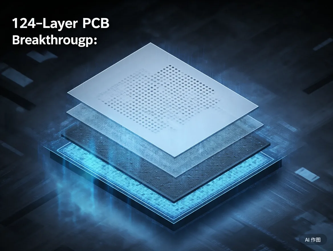
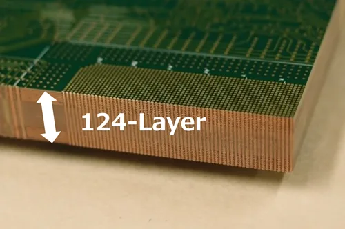
Impulsado por la inteligencia artificial (AI) y computación de alto rendimiento (HPC), the global electronics industry is undergoing a technological revolution centered on “high density, alta velocidad, and high reliability.” In May 2025, un liderazgo fabricante de PCB presentó la primera placa comercial de circuito impreso comercial de 124 capas del mundo, Romper la larga barrera de la industria de 108 capas mientras mantiene el grosor estándar de la placa de 7.6 mm. Este hito no solo proporciona soporte de hardware crítico para los servidores de IA, prueba de semiconductores, y sistemas de defensa, pero también desbloquea nuevas fronteras en la tecnología de envasado electrónico.

Rompiendo la barrera de 108 capas: Soluciones de ingeniería detrás de los PCB de 124 capas
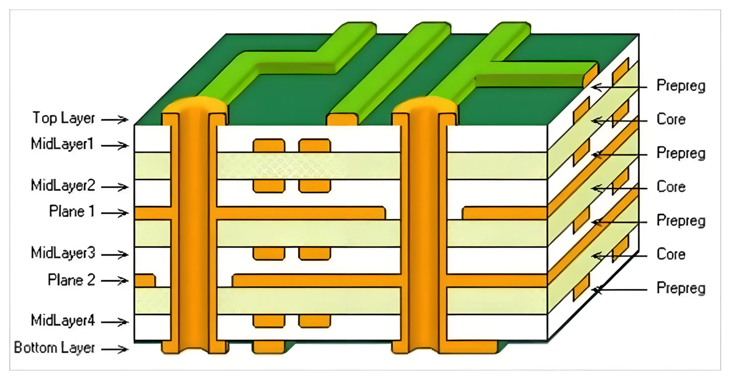
Innovaciones de fabricación de precisión
Tradicional Diseños de PCB enfrentar limitaciones mecánicas y térmicas en 100 Capas debido a inconsistencias del flujo de resina, a través del colapso, y desalineación de capas. El avance de 124 capas PCB logra un 15% Aumento de la capa a través de:
-
Dieléctricos ultra delgados: 25µm de capas utilizando materiales de baja pérdida (p.ej., Cayó 7) con ± 5% de control de impedancia para 112+ Señales de GHZ
-
3D Optimización de interconexión: Matrices de microvia que habilitan densidad de señal de 0.15 mm²/mm, Cumple con PCIe Gen6 y CXL 3.0 protocolos
Certificación de confiabilidad térmica
Certificado bajo estándares MIL-STD-883G, Las poses de PCB de 124 capas 1,000+ ciclos térmicos (-55° C a 125 ° C) mientras mantiene <1% pérdida de señal a 80 Estrés mecánico de MPA: lo hace ideal para aplicaciones aeroespaciales y de defensa.

Aplicaciones: Acelerando el hardware de IA y los avances de semiconductores
Servidores AI & Memoria de alto ancho (Hbm)
-
Densidad de señal: 18% aumento en el enrutamiento de pares diferenciales por capa
-
Gestión Térmica: Las microvias llenas de cobre mejoran la conductividad térmica por 30%, crítico para aceleradores de 500W+ AI
Prueba de nivel de obleas & 3D Embalaje
Habilita la precisión de alineación submicrónica (± 0.8 mm) y control de retraso de señal de nivel de picosegundos para módulos HBM apilados: un cambio de juego para arquitecturas basadas en chiplet.

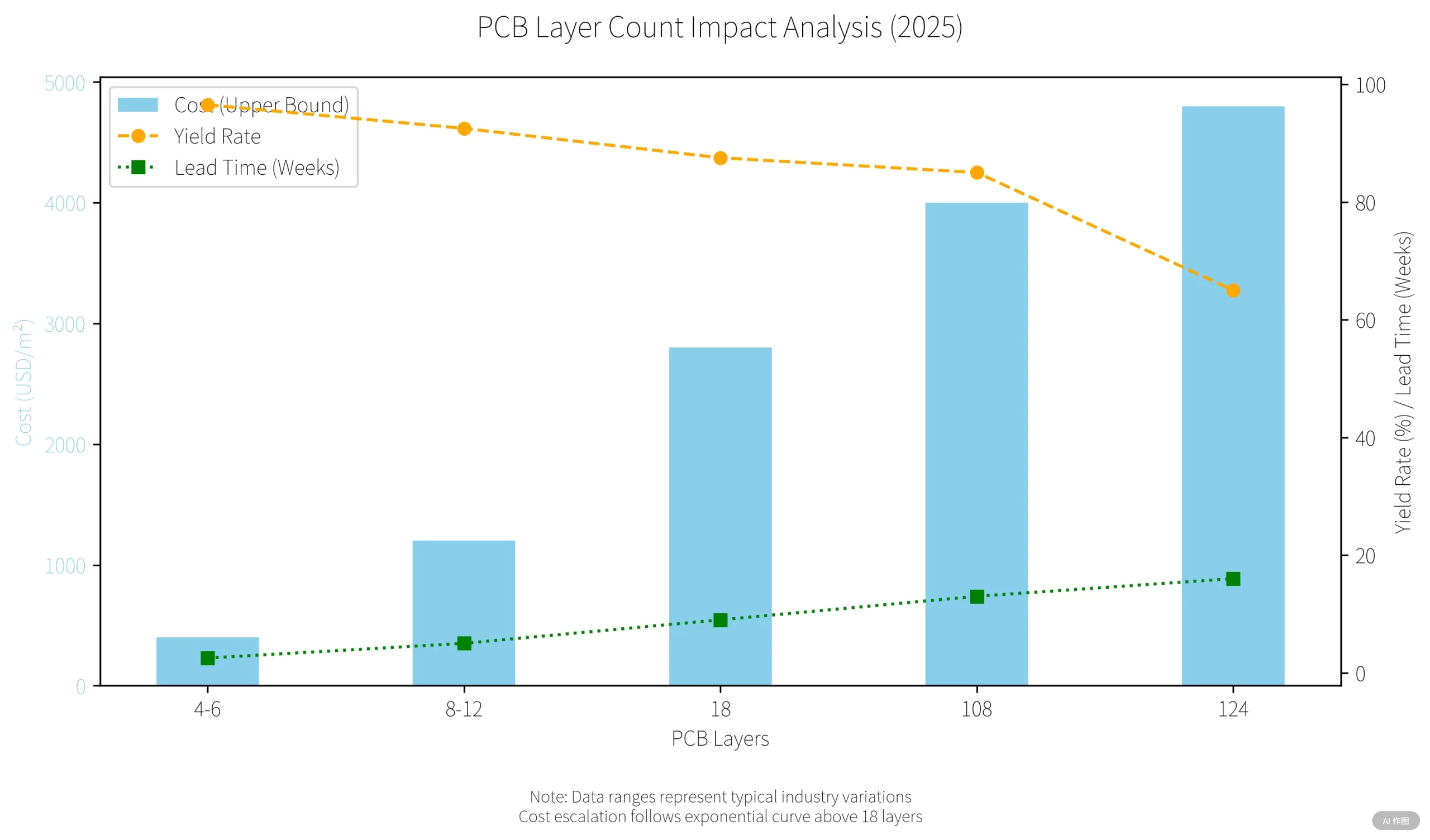
Desafíos de costos & Hoja de ruta de escalabilidad
Economía de fabricación
-
Costo de material: 4,800/M2(VS.3,200/m² para 108 capas)
-
Tasas de rendimiento: 65% (16-ciclo de la semana) VS. 85% para convencional IDH
-
Análisis de fallas: Se requiere una sección transversal destructiva para 20% de defectos de estrés térmico
Vías de adopción industrial
-
Fabricación aditiva: Reduce los pasos de laminación por 40%
-
EDA impulsada por IA: Predice a través de puntos de estrés con 92% exactitud, potencialmente aumentando los rendimientos a 75%

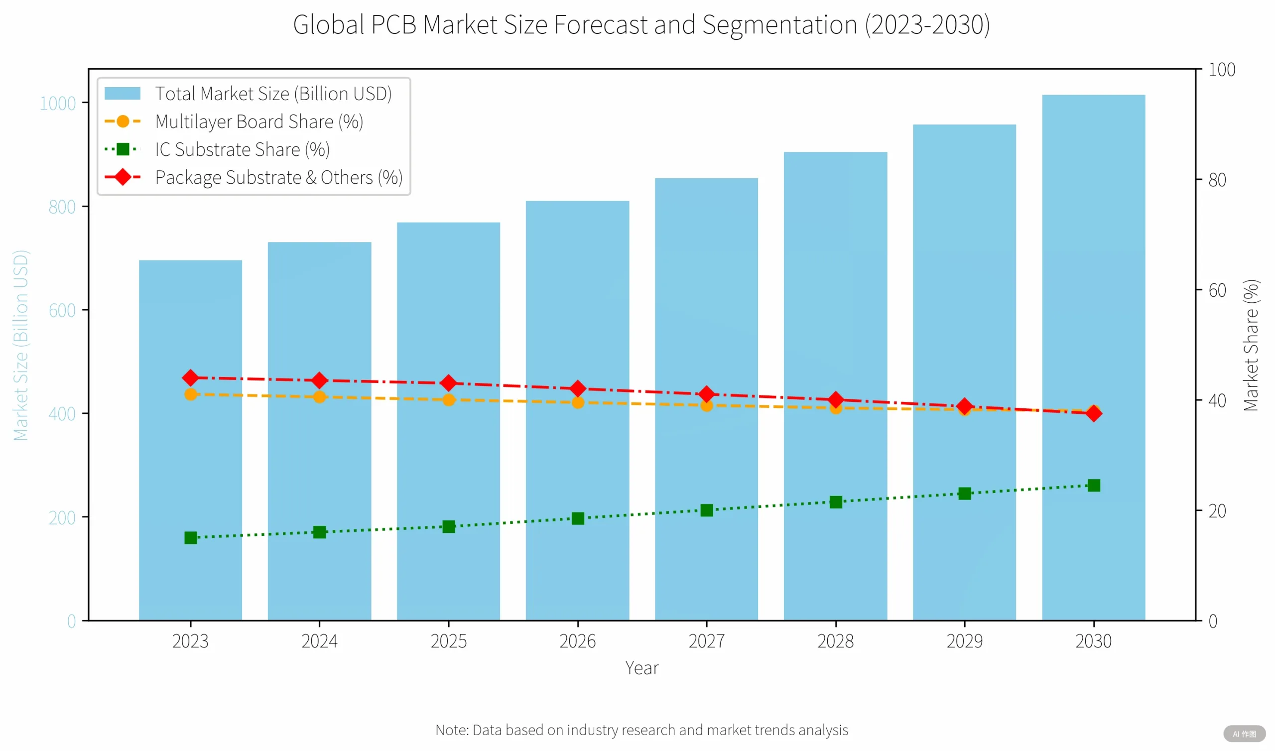
Perspectiva del mercado: $49B Transformación de la industria de PCB
Conductores de crecimiento
-
Computación en la nube: 70% CAGR en PCB del servidor AI (Valores cíticos 2026 proyección)
-
Dispositivos de AI de borde: 30% Aumento de costos de PCB en teléfonos inteligentes de próxima generación (Datos de la cadena de suministro de Apple)
-
Tendencias de localización: A los fabricantes chinos les gusta UGPCB Dirigir a 3,6 m m²/año de capacidad para sustratos avanzados

Conclusión: Innovación práctica sobre registros de recuento de capas
Aunque no supere el prototipo de 129 capas de Denso (2012), Este PCB de 124 capas establece un nuevo punto de referencia comercial:
-
Espesor estandarizado (7.6milímetros) Para la compatibilidad con atrasado
-
Confiabilidad Mil-Spec en 85% de costos prototipo
-
Procesos de fabricación escalables
A medida que emergen la computación cuántica y 6g, La innovación de PCB priorizará la densidad funcional sobre el recuento de capas: un cambio crucial para el progreso tecnológico sostenible.