

Professional Product Overview: The 12-Layer High-Speed, High-Density PCB
In the era of high-speed data transmission and complex system integration, conventional printed circuit boards (PCB) fall short of meeting the performance demands of advanced electronics. El 12-layer high-speed, PCB de alta densidad is the engineered solution. Featuring up to 12 precisely aligned conductive layers, it enables intricate interconnections and efficient signal transmission within a compact footprint, serving as the “central nervous system” for high-end networking gear, data center servers, high-performance computing (HPC), and AI hardware.
As an expert fabricante de PCB y Proveedor de PCB, UGPCB leverages advanced processes to deliver reliable 12-capa placa PCB producción, ensuring your products maintain a competitive performance edge.
In-Depth Parameter Analysis: The Foundation of Performance
The capability of a high-quality multilayer printed circuit board is defined by its specifications. Below is an analysis of this product’s core parameters:
-
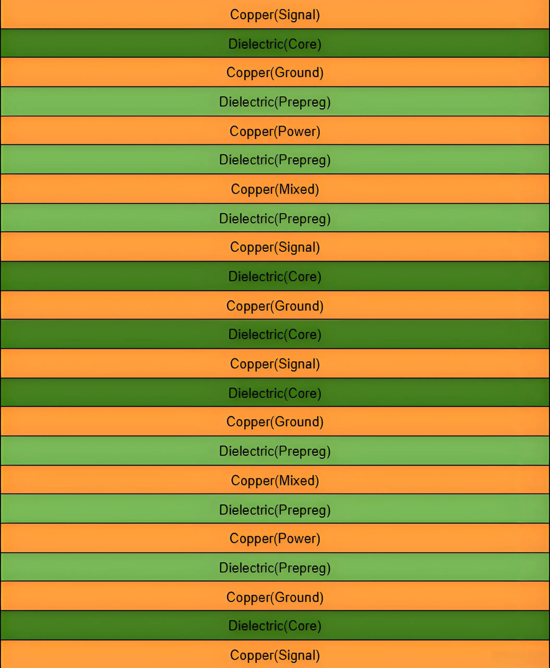
Recuento de capas & Stack-up: 12 capas. Este multilayer PCB design offers superior signal integrity (Y), integridad del poder (PI), and EMC performance compared to boards with fewer layers. It allows for dedicated power and ground planes, providing clear return paths for high-speed signals.
-
Grosor del tablero & Tolerancia: 2.4mm ±10%. This robust thickness offers excellent mechanical strength for backplanes and large-form-factor applications, ensuring reliability during mating and installation. The tight tolerance guarantees consistency in assembly.
-
Finished Copper Weight: Unique distribution:
1/1/1/1/1/2/2/1/1/1/1/1 oz. This indicates that the inner layers (L6 & L7) utilize 2oz heavy copper, designed specifically for high-current power delivery. The outer and other signal layers use 1oz copper, optimized for fine-line etching. This hybrid construction is a hallmark of alta fiabilidad fabricación de PCB. -
Critical Process Capabilities:
-
Minimum Drilled Hole Size: 0.2milímetros. Supports high-density BGA fan-out, enhancing routing flexibility.
-
Minimum Line Width/Space: 0.076milímetros / 0.09milímetros (3mil / 3.5mil). Logra Interconexión de alta densidad (IDH)-level routing, essential for high-speed signal propagation.
-
-
Acabado superficial: OSP (Conservante de soldabilidad orgánico). Compatible with both leaded and lead-free soldering, it protects copper pads from oxidation, offers excellent surface planarity, and is cost-effective—ideal for boards with dense SMT componentes.
Materiales núcleos & Key Technologies: Enabling Superior Signal Integrity
-
High-Performance Laminate: Utilizes Nanya NY6300S high-speed laminate. Its high glass transition temperature (tg >150°C) ensures dimensional stability and reliability during high-temperature reflow soldering. Its optimized dielectric constant (Dk) and dissipation factor (df) significantly reduce signal loss at high frequencies, forming the material foundation for PCB de alta frecuencia.
-
Advanced Copper Foil: Employs rtf (Reverse Treated Foil) cobre. Compared to standard electrodeposited (Edición) foil, RTF foil features a smoother, low-profile surface on the treated side. This reduces signal loss due to the “efecto piel” en altas frecuencias, critically enhancing the performance of differential signals exceeding 10 GBPS.
-
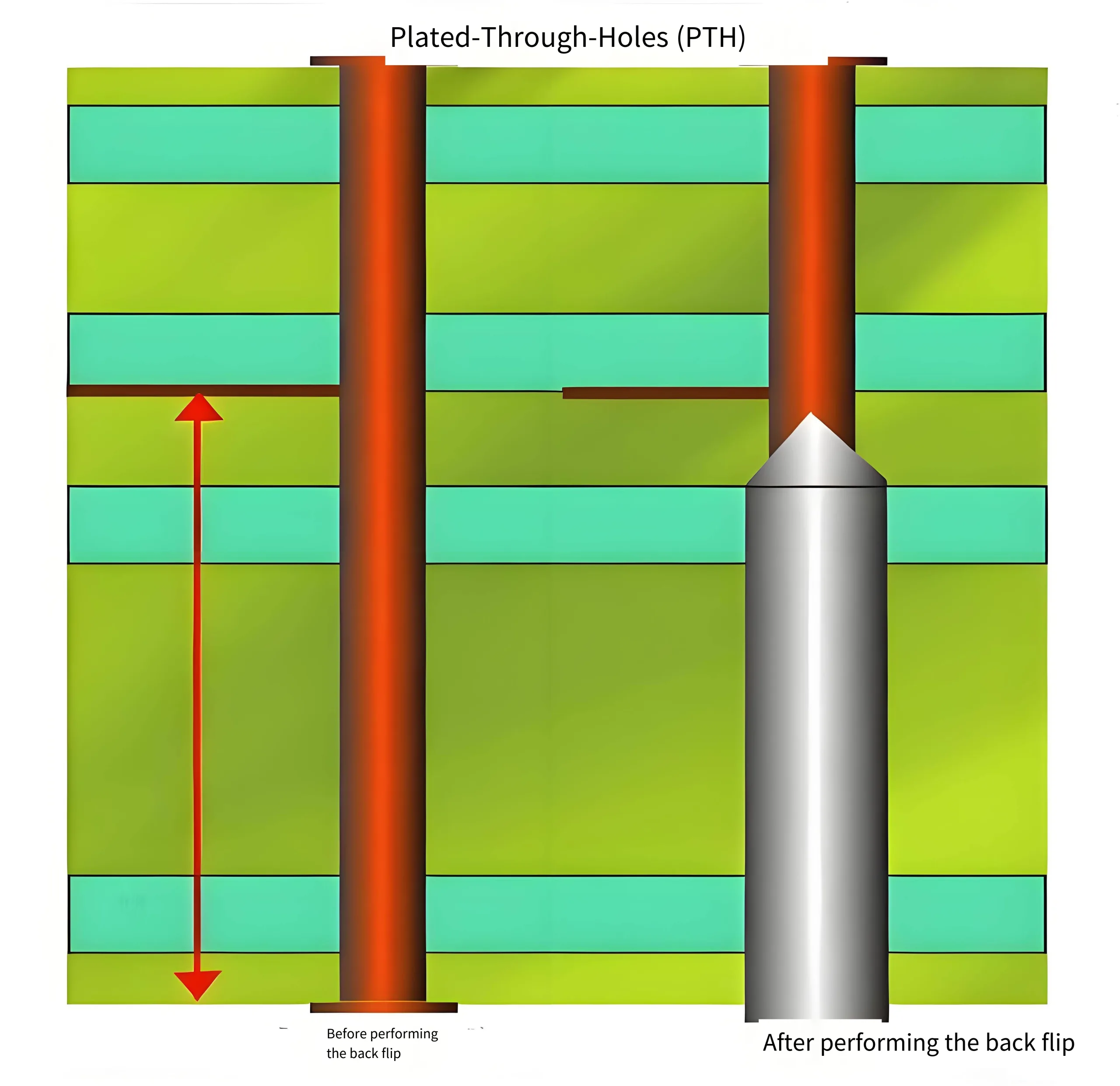
Critical Process: Controlled-Depth Drilling (Perforación trasera): In 12-layer or higher PCB multicapa, the unused portion (talón) of a through-hole via can cause significant signal reflection, degrading integrity. El back drilling process precisely removes this non-functional via stub, eliminating its negative impact—a key technology for high-speed multilayer PCB actuación.
Production Flow & Seguro de calidad
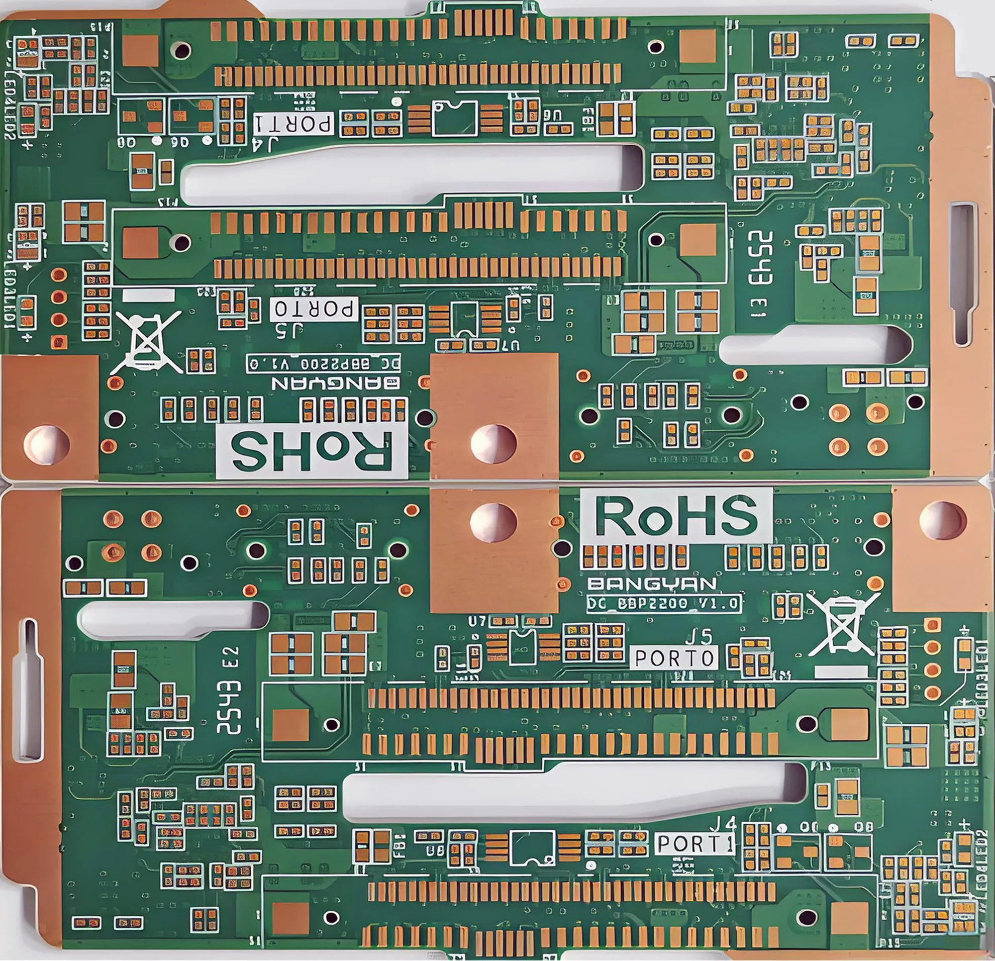
UGPCB 12-proceso de fabricación de PCB en capas strictly adheres to Normas IPC and includes Diseño para la fabricación (DFM) revisar, inner layer imaging, laminación, perforación (including back drilling), enchapado, outer layer imaging, solder mask application, acabado superficial (OSP), enrutamiento, electrical testing, e inspección final. Each stage is supported by precision measurement equipment (AOI, Impedance Testing, Prueba de sonda voladora), ensuring every tarjeta de circuitos delivered meets design specifications and our high-quality standards.
Aplicaciones típicas & Clasificación de productos
This high-performance placa PCB is designed for demanding electrical environments and complex systems, primarily used in:
-
High-End Network & Equipo de comunicación: Placas base centrales para módulos ópticos 400G/800G, enrutadores de alta gama, y cambia.
-
Data Center & Computación en la nube: Placas base de servidor, accelerator cards, placas posteriores de almacenamiento.
-
Informática de alto rendimiento: Workstation motherboards, GPU computing cards, AI accelerator hardware.
-
Advanced Test & Instrumentos de medición: Internal boards for instruments processing very high-frequency signals.
Scientific Product Classification:
-
Por recuento de capas: PCB multicapa (>8 capas)
-
By Technology Type: PCB de alta velocidad/alta frecuencia, PCB HDI, PCB de cobre pesado (partial)
-
Por aplicación: Telecom Infrastructure PCB, Data Center/Server PCB
Why Choose UGPCB for Your 12-Layer High-Speed PCB?
-
Experiencia técnica: Proven mastery of back drilling y RTF copper foil application to tackle high-speed design challenges.
-
Fabricación de precisión: Capable of 3/3.5 mil line/space, meeting stringent high-density interconnect requirements.
-
Material Integrity: Core use of reputable high-speed laminates like Nanya NY6300S ensures foundational performance.
-
Soporte de diseño: Expert diseño de PCB y DFM review services to de-risk your project from the start.
-
Consistent Quality: A fully controlled producción de PCB and inspection system delivers reliable products you can trust.
Ready to elevate your hardware? Contact UGPCB’s engineers for a free PCB quote y Análisis DFM on your next 12-layer high-speed board project.


This internet website might be a walk-through its the data you wanted in regards to this and didnt know who should. Glimpse here, and youll completely discover it.