
Introduction to IC Chip Test PCB
Descripción general y definición
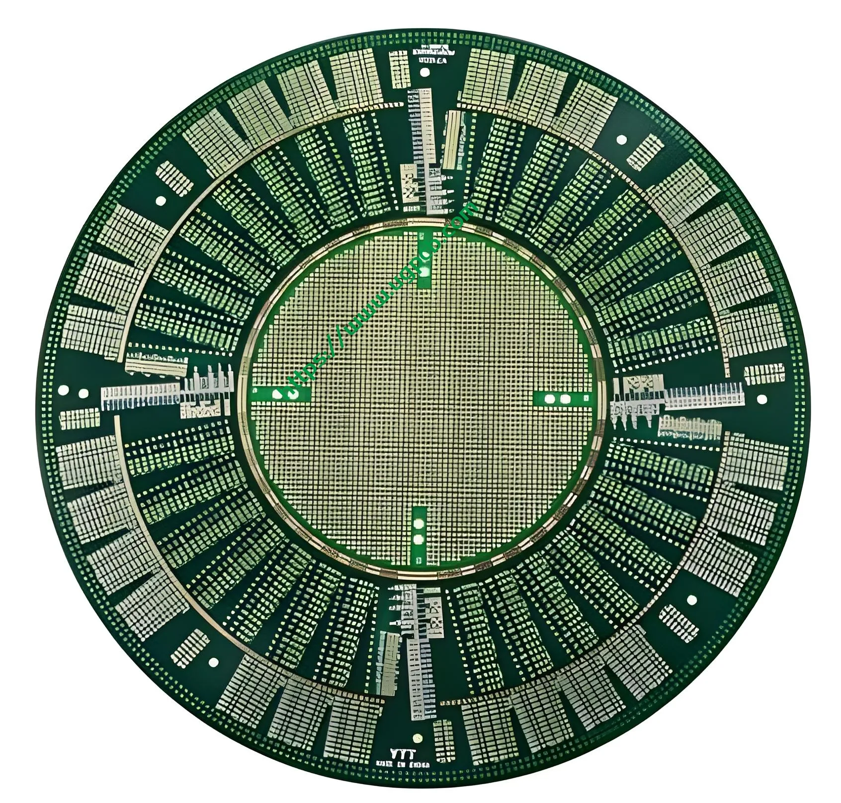
An IC Chip Test PCB, or Integrated Circuit Chip Test Placa de circuito impreso, is a specialized circuit board designed for testing integrated circuit chips. It ensures that the chips meet the required specifications before they are used in electronic devices.

Principio de trabajo
The IC Chip Test PCB works by connecting the integrated circuit chip to various test points on the tarjeta de circuito impreso. These test points measure the electrical characteristics of the chip, such as voltage, actual, and resistance, to verify its functionality.
Aplicaciones
IC Chip Test PCBs are used in the manufacturing and quality control processes of electronic devices. They are essential for ensuring that only functioning and reliable chips are used in the final products.


Types of IC Chip Test PCBs
There are different types of IC Chip Test PCBs based on their design and functionality:
- Functional Test PCBs: Used to test the overall functionality of the chip.
- Parameter Test PCBs: Used to measure specific parameters like power consumption, velocidad, and temperature.
Material y construcción
- Material: TU872SLS, un material epoxi de alta calidad.
- capas: 20 capas, proporcionando robustez y una mejor integridad de la señal.
- Color: Disponible en verde o blanco.
- Espesor terminado: 2.0milímetros, asegurando durabilidad y al mismo tiempo siendo delgado.
- Espesor de cobre: 1ONZ, que ofrece buena conductividad.
- Tratamiento superficial: Immersion gold with a thickness of at least 3U”, mejorando la resistencia a la corrosión y la soldabilidad.
Características de rendimiento
IC Chip Test PCBs are designed to accurately test the performance of integrated circuit chips. They support high-speed data transfer and are built to withstand repeated usage over time. El acabado dorado por inmersión garantiza un rendimiento y una fiabilidad duraderos..
Características estructurales
The structure of an IC Chip Test PCB includes multiple layers of copper traces sandwiched between layers of substrate material. Este diseño multicapa ayuda a gestionar la disipación de calor y mejorar el rendimiento eléctrico.. The PCB is coated with a protective layer to prevent damage and ensure longevity.
Proceso de producción
The production of an IC Chip Test PCB involves several steps:
- Diseño: Usar software especializado para crear el diseño del circuito..
- Aguafuerte: Quitar el exceso de cobre para formar los patrones deseados..
- Laminación: Combinando varias capas juntas.
- Enchapado: Agregar una fina capa de metal para mejorar la conectividad.
- Inspección: Garantizar que la PCB cumpla con los estándares de calidad.
- Asamblea: Montaje de componentes en la PCB.
- Pruebas: Verificación de funcionalidad y rendimiento.


Casos de uso
IC Chip Test PCBs are used in various applications including:
- Electrónica de Consumo: Teléfonos móviles, tabletas, relojes inteligentes.
- Automotor: In-car systems for navigation and entertainment.
- Dispositivos médicos: Equipo médico portátil.
- Automatización industrial: Control systems for machinery and robotics.
En conclusión, IC Chip Test PCBs play a crucial role in the electronics manufacturing process by ensuring the reliability and functionality of integrated circuit chips. Su adopción generalizada en diferentes industrias resalta su versatilidad e importancia en los dispositivos electrónicos modernos..