

A mere 0.5mm² crack in a BGA solder pad can brick a premium smartphone into a “white-screen paperweight” – while conventional underfill encapsulation merely disguises this critical PCB reliability threat. Alors que les smartphones évoluent rapidement vers des conceptions ultra-minces et des spécifications hautes performances, Craquage BGA has become the Damocles’ sword hanging over PCB fabrication. Quand un $1,000+ téléphone mobile Assemblage de circuits imprimés devient une ferraille en raison de micro-fissures ou de surtension de taux de retour sur le marché 30% depuis Fractures de type V, Nous devons demander: Est sous-rempli la solution ultime?
1. Craquage BGA: Le tueur invisible de l'électronique
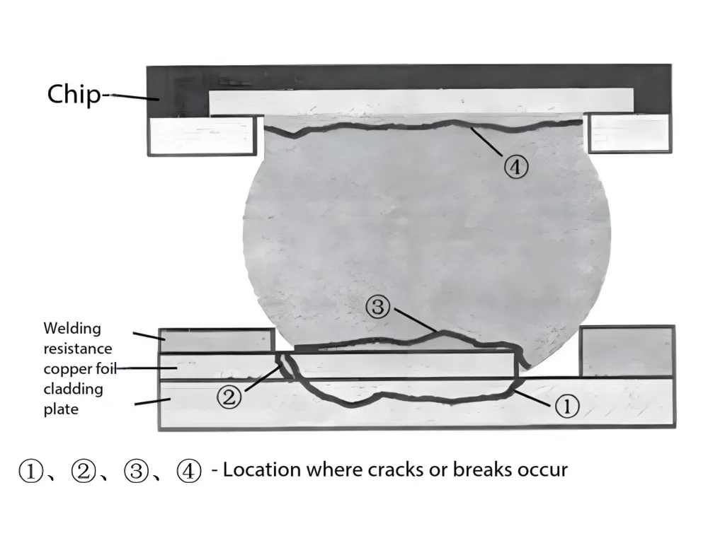
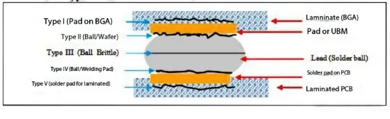
H3: 1.1 Définition de l'échec & Cinq types de fracture
Craquage BGA fait référence à la séparation entre Puces ic et coussinets de PCB sous contrainte mécanique / thermique. Cinq types de fracture sont classés par emplacement:
| Taper | Emplacement de défaillance | Prévalence | Déclencheurs primaires |
|---|---|---|---|
| Type I | Substrat de puce couche | 12% | Tests de tumbling, choc mécanique |
| Type II | Interface BGA Pad-Solder | 18% | Cyclisme thermique |
| Type III | Balle de soudure sans plomb | 25% | Impact, choc thermique |
| Type IV | Joint de coussinet Solder-PCB | 28% | Déliachance de profil de reflux |
| Type V | Séparation de pad-substrat | 17% | Déformation structurelle, dégradation des matériaux |

1.2 Nature furtive & Impact destructeur
L'inspection SMT traditionnelle détecte <5% de fissures de pad en raison de:
-
Tailles de micro-crack (5-50µm) obscurci dans les PCB multicouches
-
La continuité électrique souvent maintenue malgré les fractures
-
Masques sous-remplies fissures sans interrompre la propagation, nécessiter un retrait destructeur lors de reprise


2. Analyse des causes profondes sur le flux de travail PCBA
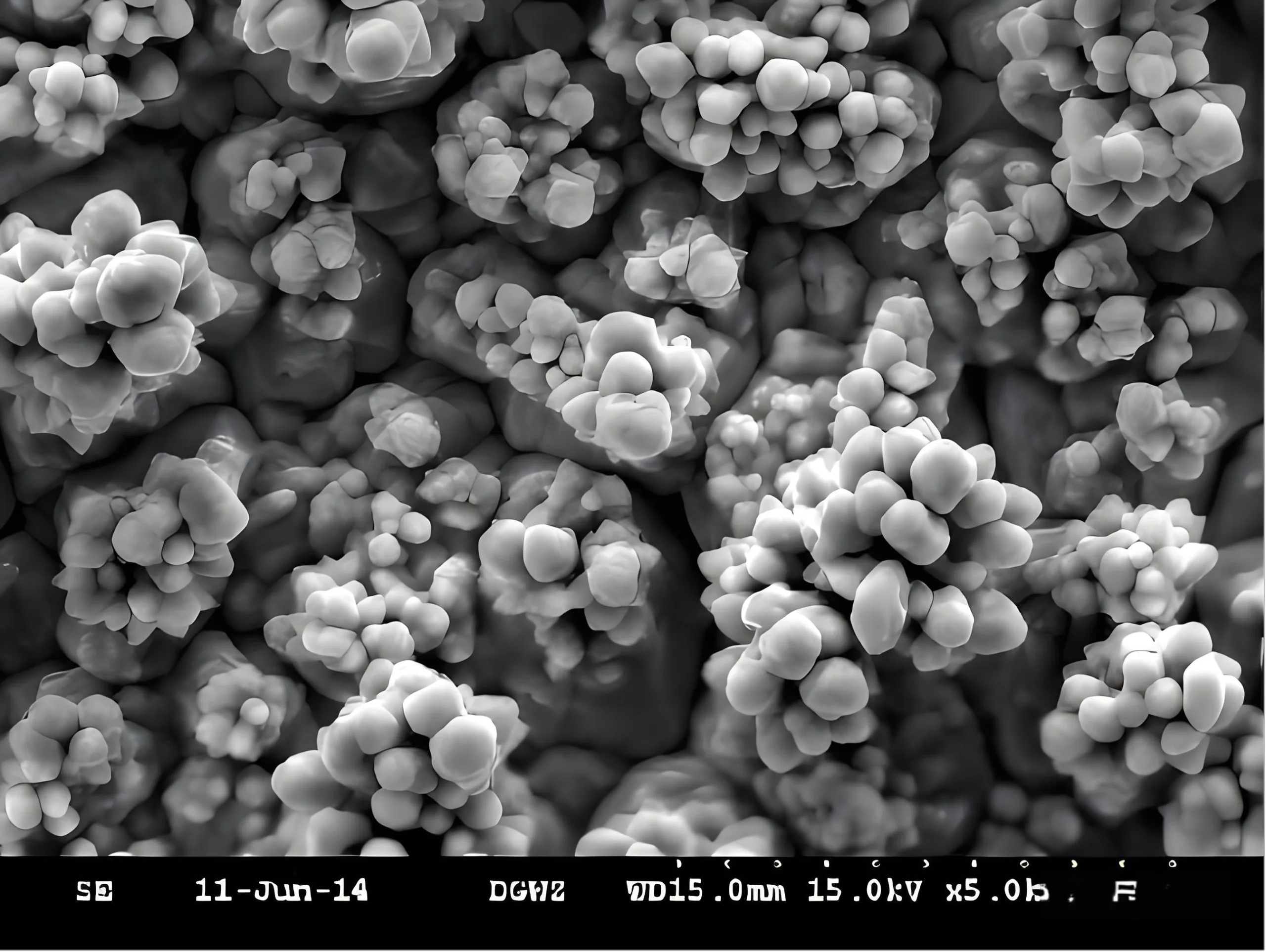
2.1 Origine: Structure cristalline en feuille de cuivre Divergence
Les données expérimentales révèlent: Copper foil with specialized “grape-like” nodular structures delivers 18.5% Adhésion plus élevée que les cristaux conventionnels.

2.2 Substrat PCB Limites: Crise d'endurance thermique du FR4
Le soudage sans plomb exige des températures maximales de 248 ° C (+33° C vs processus traditionnels). FR4 standard Tg de 130-140 ° C causes:
-
Axe Z CTE >300 ppm/°C
-
Temps de délaminage T288 <3 min (L'industrie exige >5 min)
Formule critique: Contrainte thermique = e × α × Δt
Où:
σ = contrainte thermique (MPA), E = module élastique (GPA),
α = cte (ppm/°C), Δt = changement de température (° C)
*Les substrats de CTE élevé génèrent 1,8 × plus de contrainte à Δt = 100 ° C *
2.3 Conception de circuits imprimés Écrans: Contrainte mécanique négligée
Analyse de 7,000 Échec des unités sur les marchés russes montrent:
-
0.80Les planches MM ont échoué 3,2 × plus de 1,00 mm
-
Les machines à sous en T 47%
-
De grands composants dans les zones BGA ont provoqué une déformation thermique asymétrique
3. Percères de contrôle des processus PCB critiques
3.1 Matrice d'optimisation de la fabrication de PCB
| Processus | Conventionnel | Optimisé | Amélioration |
|---|---|---|---|
| Feuille de cuivre | Nodules standard | Cristaux de raisin | Adhésion ↑ 18,5% |
| Épaisseur | 18-23µm | ≥30 μm | Traction ↑ 32% |
| Préparation de surface | Ponçage de ceinture | Micro-gravure + pulvérisation | Perte de cuivre ↓ 60% |
| Ouverture du masque de soudure | Circulaire | Hexagonal | Flux de pâte ↑ 40% |
3.2 Révolution du profil de reflux
Racine de défaillance: La reflux standard ne passe que 12 s refroidissement à partir de 190 ° C → 130 ° C, provoquant une contraction rapide.
Solution: Prolongez le temps de séjour au-dessus de TG par 150%, réduisant la contrainte thermique par 35%.
4. Base de données complète des solutions PCBA
4.1 Innovations de conception
-
Géométrie du pad: Convertir les coussinets périphériques en ovale (axe long + 0,1 mm)
-
Conception d'empilement: Ajouter des couches de bilan de cuivre localisées sous BGAS
-
Règle d'autorisation: Interdire grand composants à moins de 3 mm des zones BGA
4.2 Chemin de mise à niveau des matériaux
-
Spécifiez FR4 avec TG ≥170 ° C
-
Contrôler la feuille de cuivre RZ (rugosité) à 3,5-5,0 μm
-
Adopter le bas-CTE (<2.5%) Systèmes de résine à hauteur
4.3 Contrôle de processus Redlines
-
Placage en cuivre ≥30 μm (validé)
-
Espacement du panneau OSP >5mm (Prévention du piégeage d'acide)
-
Pression du luminaire de test ≤7 kg / cm², épingler la vie <500k cycles
-
150-180° C Zone de reflux habitant ≥90 secondes
5. Feuille de route future
Comme PCB HDI Avancez vers 0,4 mm d'épaisseur et les coussinets BGA se rétrécissent en dessous de 0,2 mm, percées requises:
-
Traitement de cuivre nano-échelle: Couches d'adhésion à bache-magnétron
-
Substrats adaptatifs du CTE: Composites polymères sensibles à la température
-
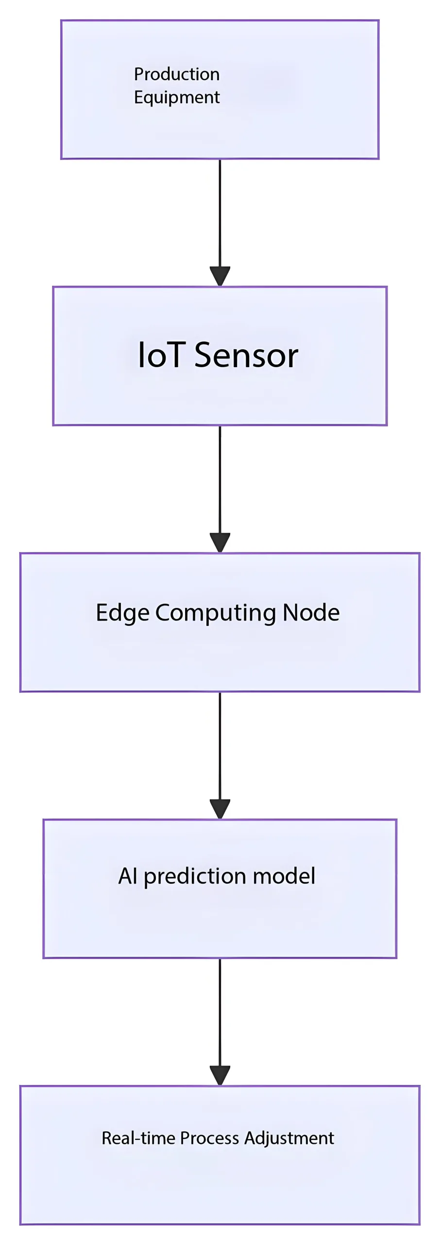
Surveillance du processus d'IA: Prédiction conjointe de la soudure en temps réel

Conclusion: La fiabilité est conçue dans
La fissuration du pad BGA constitue Échec de la fiabilité au niveau du système. Résultats post-mise en œuvre:
-
Taux de réussite des tests de tumbling: 82% → 99.6%
-
Taux de rendement du marché: ↓ 70%
-
Réduction des coûts: $1.20/Board via l'élimination de la sous-tension
*Souviens-toi: Une augmentation de 0,1 kgf de l'adhésion par pad offre des gains de fiabilité exponentiels. Cela transcende le raffinement du processus - il incarne la poursuite ultime de la fabrication à défaut zéro. *
Dans le domaine microscopique des coussinets de soudure, Les cristaux de cuivre en forme de raisin tissent les réseaux de protection nano-échelle, tandis que les sphères sans plomb effectuent des danses de précision dans les ouvertures du masque hexagonal. La révolution de la fiabilité de l'électronique commence par un engagement indéfectible à chaque 0,01 mm.