

In the era of high-speed data transfer and precision computing, the performance of the circuit imprimé (PCB)—the core brain of electronic devices—determines the entire system’s capability. UGPCB introduces its high-performance 18-PCB rigide en couche basé sur Megtron-7 matériel, engineered to meet the most demanding electrical and physical challenges, serving as the essential foundation for your next-generation advanced equipment.
1.18-Layer Megtron-7 Rigid PCB Présentation du produit & Définition
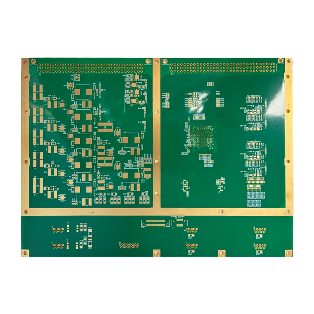
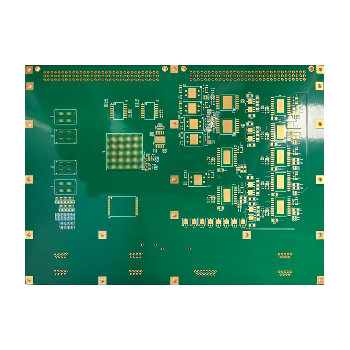
Ce produit est un 18-layer rigid high-layer count PCB with a precisely controlled thickness of 1.86mm and overall dimensions of 165mm x 120mm. It utilizes industry-leading Megtron-7 high-speed low-loss laminate and features a 2-microinch (environ. 0.05µm) Or par immersion au nickel autocatalytique (ACCEPTER) finition de surface. This specification represents an advanced tier in haute performance Fabrication de PCB, designed for applications where signal integrity, gestion thermique, and reliability are paramount.

2. Considérations critiques de conception
Designing a successful 18-layer PCB, especially with high-speed materials like Megtron-7, requires careful attention to several core aspects:
-
Stack-up Design: A rational layer stack-up is critical for impedance control and crosstalk reduction. A typical 18-layer stack includes multiple signal, pouvoir, and ground planes to ensure stable power distribution and clear signal return paths.
-
Contrôle de l'impédance: High-speed signal transmission demands precise PCB à impédance contrôlée conception. Trace width and spacing must be calculated accurately based on the Dk (Constante diélectrique) et Df (Facteur de dissipation) of Megtron-7. We offer professional impedance calculation and simulation services.
-
Gestion thermique: The 1.86mm board thickness and multi-layer structure necessitate effective thermal pathways in the design, such as using thermal vias to connect internal copper layers for efficient heat dissipation from components.
-
Interconnexion à haute densité (IDH) Considérations: While this is a standard through-hole design, careful planning of via types (blind, enterré, through-hole) is essential at this layer count to minimize stub effects and optimize signal paths.
3. Comment ça marche & Structure
UN PCB multicouche functions like a highly integrated, three-dimensional “road network.” Electrical signals travel on copper traces (“roads”) on the surface and internal layers, with vertical connections between layers established through plated through-holes (“interchanges”). Dedicated power and ground planes provide stable voltage reference and noise shielding for the entire system. Ce 18-PCB rigide en couche is formed through a precise lamination process, bonding multiple core layers and prepreg sheets into a single, robust unit with excellent electrical properties. Its sophisticated PCB board structure is the foundation for implementing complex circuit functionalities.
4. Matériaux de base & Key Performance
-
Matériaux utilisés:
-
Stratifié: Megtron-7. This is a high-performance, low-loss copper-clad laminate from Panasonic, renowned for its stable dielectric constant (Dk ~3.3) and extremely low dissipation factor (Df ~0.001). It is optimized for applications above 10GHz and into millimeter-wave frequencies.
-
Feuille de cuivre: Utilizes Very Low Profile (VLP) or Reverse Treated Foil (RTF) to minimize “skin effect” losses caused by signal transmission on rough copper surfaces.
-
Finition de surface: Or par immersion au nickel autocatalytique (ACCEPTER, 2u”). Provides a flat surface, excellente soudabilité, a reliable contact interface (suitable for gold fingers), et longue durée de conservation.
-
-
Outstanding Performance:
-
Intégrité supérieure du signal (ET): Exceptionally low signal loss ensures high-speed pulse waveforms remain undistorted.
-
Excellent Power Integrity (PI): Multiple dedicated power and ground planes offer very low power distribution network impedance and superior decoupling.
-
Haute fiabilité: The 1.86mm board thickness and premium materials deliver high mechanical strength, résistance à la chaleur, and long-term environmental stability.
-
Stable Impedance Control: Achieved through material consistency and precision manufacturing processes.
-
5. Classement du produit
According to industry and IPC standards, this product is accurately classified as:
-
Par nombre de couches: High-Layer Count PCB (typically defined as 10+ couches).
-
Par type de matériau: High-Speed High-Frequency PCB / Low-Loss PCB.
-
Par structure: PCB rigide.
-
Par technologie: Controlled Impedance PCB, ENIG Finished PCB.
-
By Application Grade: Industrial Grade / Telecommunications Grade High-Performance PCB.
6. Caractéristiques clés & Avantages
-
Premium Material: Built on Megtron-7 high-speed laminate, providing the physical basis for superior electrical performance.
-
High Complexity Capacity: Le 18-carte de circuit imprimé de couche design allows for extremely complex and dense circuit layouts.
-
Fabrication de précision: Strict tolerance control on the 1.86mm board thickness and consistent 2u” ENIG surface finish application.
-
Engineered for Speed: Optimized throughout—from design and material selection to processing—for high-speed digital circuits et RF/microwave circuits.
7. Aperçu du processus de production
Le high-layer count PCB manufacturing process is highly precise: Material Cutting → Inner Layer Imaging & Etching → Automated Optical Inspection (Zone d'intérêt) → Lamination (Pressing multiple inner layer cores with prepreg) → Drilling → Hole Metallization (Désenduire, Electroless & Electrolytic Copper Plating) → Outer Layer Imaging → Pattern Plating → Etching → Solder Mask Application → Surface Finish (ACCEPTER) → Profile Routing → Electrical Testing → Final Inspection. Each step requires stringent control, particularly layer-to-layer registration and impedance control.
8. Applications principales & Cas d'utilisation
Ce high-performance PCB board is the ideal choice for the following advanced applications:
-
High-Speed Communication Equipment: Core motherboards for 400G/800G optical modules, high-end routers, and switches.
-
Advanced Computing & Stockage: Server motherboards, AI accelerator cards, high-speed storage array (SSD) controller boards.
-
Precision Test & Instruments de mesure: Internal core boards for high-end oscilloscopes, analyseurs de spectre, and signal generators.
-
Aérospatial & Defense Electronics: Processing units within radar systems and satellite communication payloads.
-
Advanced Medical Imaging Devices: High-speed data acquisition and processing boards for equipment like MRI and CT scanners.


Why Choose UGPCB for Your 18-Layer Megtron-7 PCBs?
We deliver more than just a circuit imprimé; we provide a complete solution encompassing DFM (Conception de la fabrication) revoir, fabrication de précision, et tests de fiabilité. We possess deep expertise in every detail of nombre de couches élevées Fabrication de circuits imprimés, ensuring your design is translated into reality with the highest quality and reliability.
Contactez-nous aujourd'hui for a free technical assessment and a competitive quote for your project. Let UGPCB be the robust foundation for your high-end product’s success.