

Révolutionner la fabrication de PCB: UGPCB’s Advanced Inner Layer Pre-Treatment Line
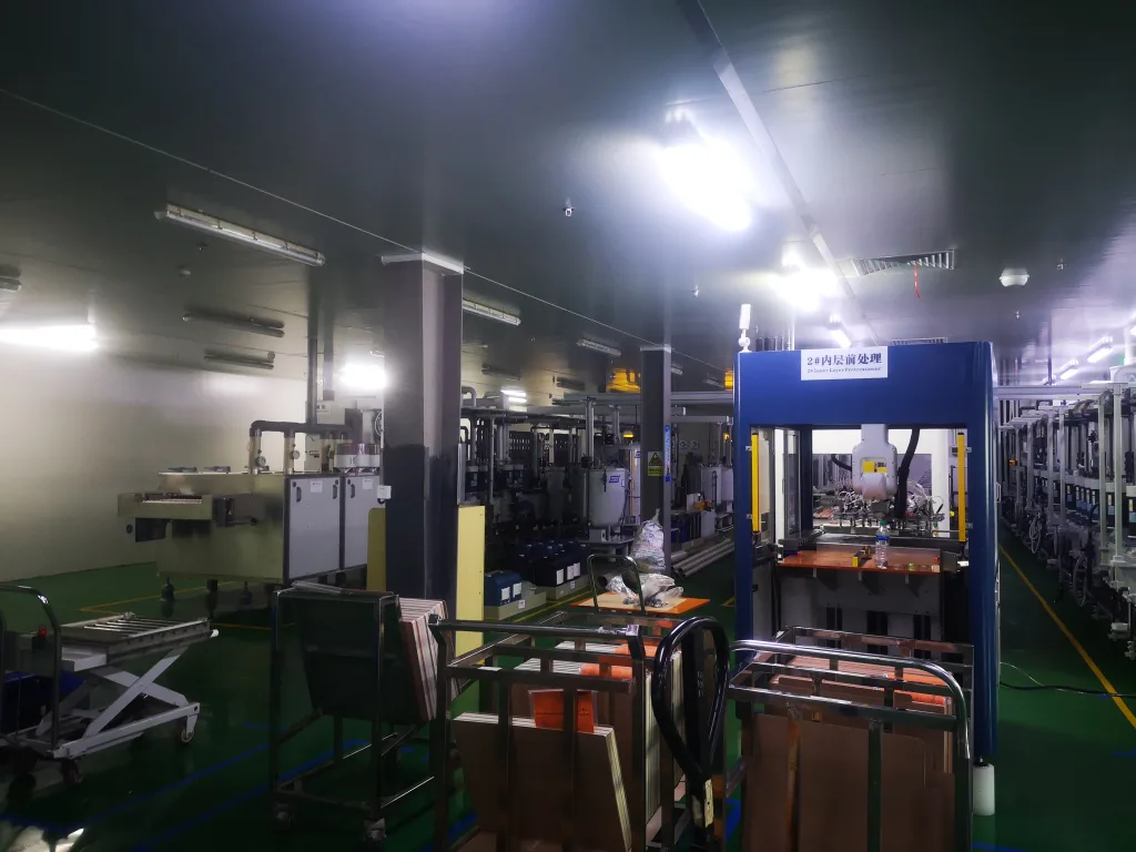
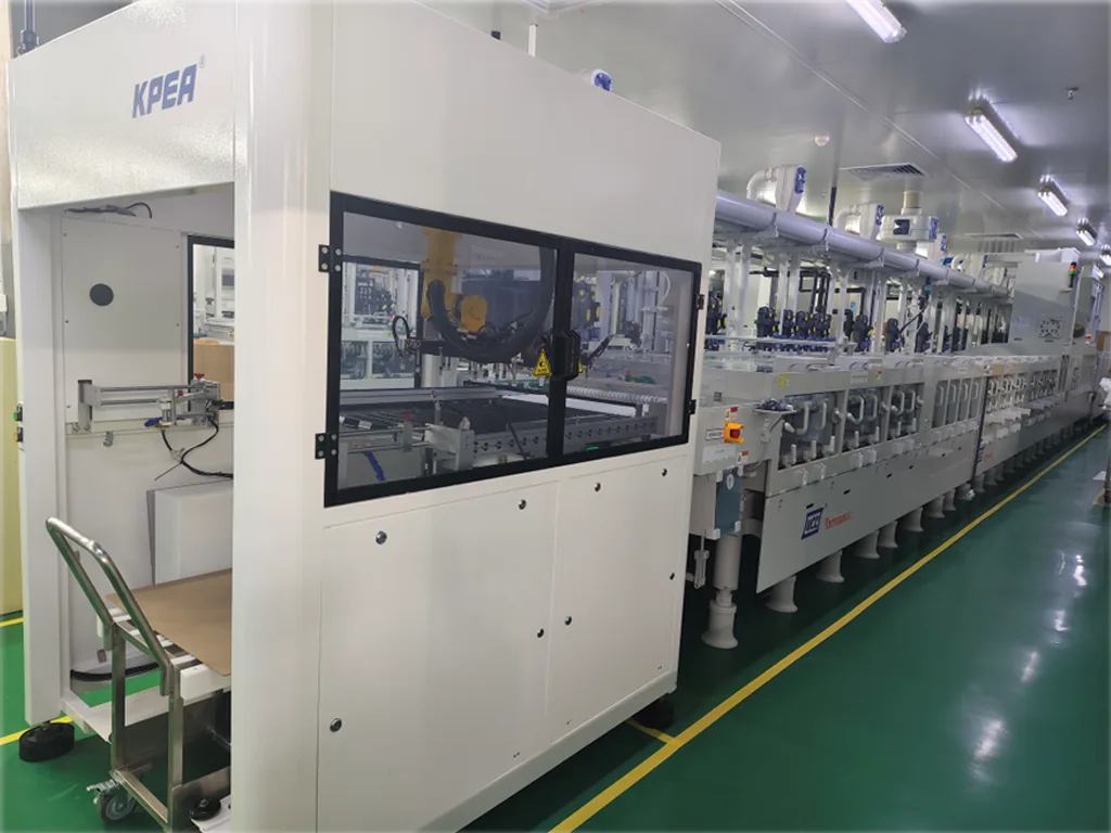
In the highly competitive world of PCB and PCB fabrication, UGPCB continues to demonstrate its commitment to excellence through strategic technological investments. Our latest advancement—a state-of-the-art PCB inner layer pre-treatment line—represents a significant leap forward in manufacturing capability and quality assurance. This fully automated system enhances our multilayer PCB production capacity while delivering unprecedented precision for today’s most demanding electronic applications.
The Critical Role of Inner Layer Pre-Treatment in PCB Manufacturing
The foundation of any reliable carte PCB multicouche begins with impeccable inner layer preparation. This stage transforms raw copper-clad laminates into precisely defined circuit patterns that will form the internal nervous system of the final board. Traditional pre-treatment methods often involved manual handling, inconsistent processing parameters, and variable results that compromised PCB reliability.
UGPCB’s new pre-treatment line addresses these challenges through comprehensive automation and precision engineering. As industry research indicates, improper surface preparation accounts for approximately 23% of inner layer defects in conventional PCB manufacturing processes . Our advanced system virtually eliminates these concerns through controlled, repeatable processes that set new standards for PCB quality control.
Technical Breakdown: UGPCB’s Inner Layer Pre-Treatment Line
Automated Material Handling and Surface Preparation
The journey begins with UGPCB’s fully automated loading and transfer system, which eliminates human contact with panels until the process is complete. This automated handling prevents the copper foil scratches that traditionally account for 5-7% of yield loss in semi-finished circuit boards .
Key Components and Parameters:
-
Robotic transfer vehicles with vacuum end-effectors ensure scratch-free panel movement
-
Integrated temporary storage racks buffer panels between processes, optimizing flow
-
Advanced brushing systems feature multi-directional brushing with diamond-embedded rollers
-
Precision micro-etching maintains copper surface roughness at 0.3-0.5 μm for optimal dry film adhesion
The micro-etching process utilizes a scientifically formulated chemical bath that achieves a consistent etch rate of 1.2-1.5 µm/min, with the removal depth precisely calibrated according to the equation:
h = k × t × C
Where h represents copper removal depth (µm), t is immersion time (minutes), C denotes chemical concentration (mol/L), and k is the reaction rate constant specific to our formulation .
Precision Cleaning and Surface Activation
Following mechanical abrasion, panels undergo a multi-stage cleaning process that combines chemical and physical methods:
-
Alkaline cleaning at 55°C removes organic contaminants
-
High-pressure spraying (20-25 kg/cm²) dislodges particulate matter
-
Overflow rinsing with deionized water ensures chemical residue removal
-
Ultrasonic immersion eliminates sub-micron particles from micro-roughnesses
This comprehensive approach reduces surface contamination to less than 0.01 μg/cm² as measured by ion chromatography, far exceeding the IPC standard of 1.56 μg NaCl/cm² for Class 3 PCB .
Advanced Drying and Moisture Control
The final stage of pre-treatment employs a multi-zone drying system that progressively removes moisture without creating thermal shock. The process maintains precise temperature gradients that never exceed 3°C/second, preventing substrate stress that can lead to future dimensional instability.
Supériorité technique: Comparative Analysis
To fully appreciate the advancements embodied in UGPCB’s inner layer pre-treatment line, consider this comparative analysis of key performance metrics:
| Paramètre | Traditional Pre-treatment | UGPCB Advanced System | Amélioration |
|---|---|---|---|
| Surface Roughness Control | ±0.2 μm | ±0.05 μm | 400% more consistent |
| Defect Rate | 5-7% | 0.5-0.8% | 85% réduction |
| Process Stability (CPK) | 1.2-1.5 | 2.2-2.5 | 80% more capable |
| Energy Consumption | 100% baseline | 65-70% | 30-35% réduction |
| Manual Handling | 3-4 transfers | Fully automated | 100% réduction |
Enhancing PCBA Performance Through Superior Inner Layers
The benefits of UGPCB’s advanced PCB inner layer pre-treatment extend throughout the manufacturing process and ultimately enhance the performance of completed PCBA assemblies. Properly prepared inner layers deliver:
Improved Impedance Control
With surface uniformity optimized through our pre-treatment process, contrôle d'impédance tolerances of ±5% are consistently achievable, even in high-speed designs with differential pairs exceeding 10 Gbit/s .
Enhanced Layer-to-Layer Registration
The dimensional stability of properly treated inner layers translates to superior registration throughout lamination. UGPCB’s process maintains layer-to-layer alignment within 25μm, enabling higher PCB layer counts without sacrificing yield .
Superior Thermal Reliability
By eliminating microscopic contaminants that can initiate delamination, UGPCB’s pre-treated inner layers withstand the rigorous thermal cycling required in automotive and aerospace PCBA applications. Our boards consistently pass 1000 cycles of -55°C to 125°C thermal shock testing without failure.
Quality Assurance and Process Validation
UGPCB’s commitment to quality is embedded throughout the pre-treatment process. Our system incorporates:
-
Real-time monitoring of chemical concentrations and temperatures
-
Automated optical inspection at critical process points
-
Statistical process control with immediate feedback loops
-
Comprehensive data logging for full traceability
This rigorous approach ensures that every panel entering our multilayer PCB production process meets the exact same high standards, resulting in exceptional consistency across small-batch prototypes and volume production runs.
Applications Across PCB and PCBA Solutions
The precision afforded by UGPCB’s inner layer pre-treatment line benefits virtually all PCB and PCBA applications, with particular advantages for:
Interconnexion à haute densité (IDH) PCB
UGPCB’s pre-treatment process enables the fine-line circuitry essential for HDI PCB designs avec 3/3 mil line/space requirements. The uniform surface topography prevents developmental issues in stacked microvia structures .
High-Frequency and RF PCBs
The controlled surface profile minimizes skin effect losses at microwave frequencies, making UGPCB’s process ideal for RF PCBA applications in 5G infrastructure and automotive radar systems .
High-Reliability Applications
For medical, militaire, et l'automobile PCBA assemblies, the exceptional cleanliness achieved through our pre-treatment process ensures long-term reliability in demanding operating environments.
L'avantage UGPCB: Beyond Equipment
While our advanced inner layer pre-treatment line represents a significant technological achievement, it is the integration of this equipment with UGPCB’s comprehensive PCB and PCBA manufacturing expertise that delivers maximum value to our clients. This synergy enables:
Design for Manufacturing Optimization
Notre PCB engineering team leverages intimate knowledge of the pre-treatment process capabilities to optimize designs for manufacturability and performance, reducing time-to-market for new products.
Seamless Process Integration
The pre-treatment process is perfectly tuned to interface with subsequent processes in our automated flow, including laser direct imaging, precision etching, et Zone d'intérêt verification.
Technical Collaboration
UGPCB partners with clients throughout the PCB and PCBA development process, providing insights that leverage our advanced capabilities to enhance product performance and reliability.
Conclusion: Setting New Standards in PCB Manufacturing
UGPCB’s investment in advanced inner layer pre-treatment technology reflects our unwavering commitment to delivering superior PCB and PCBA solutions. This state-of-the-art system ensures that every multilayer circuit board begins with a perfect foundation, enabling the exceptional performance and reliability demanded by today’s most challenging applications.
From prototype to production, UGPCB provides the technological capabilities, manufacturing expertise, and quality focus that leading electronic manufacturers require. Our integrated approach to PCB and PCBA manufacturing delivers measurable benefits in performance, fiabilité, and total cost of ownership.
Discover the UGPCB difference – contact our technical team today to discuss how our advanced inner layer pre-treatment capabilities can enhance your next PCB or PCBA project.