
The Art and Science of PCB Design: How UGPCB Masters Circuit Board Alchemy
(Engineering Excellence from Schematic to Functional PCBA)

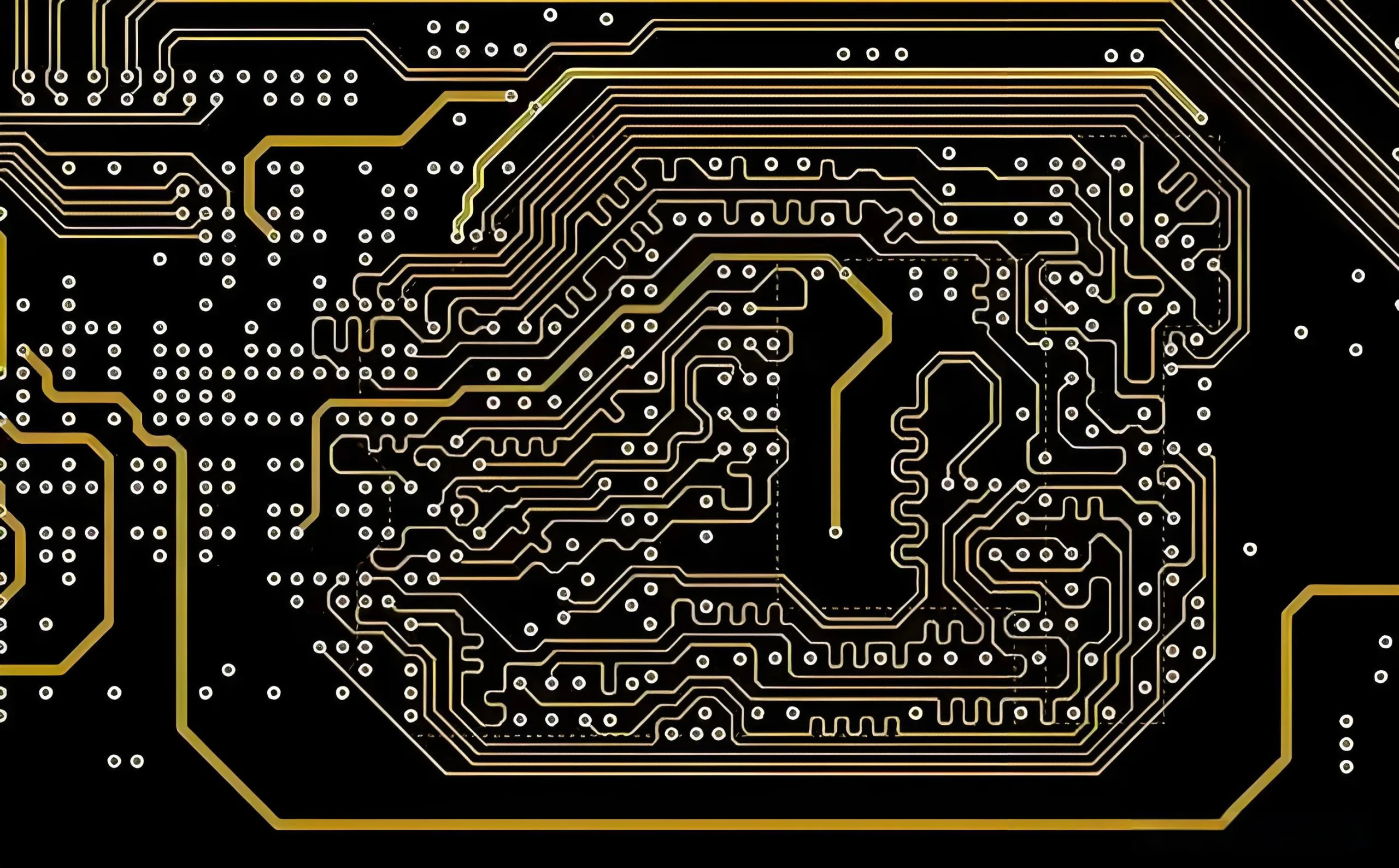
A single misplaced via on a 12-layer server motherboard once cost a tech giant $2.3 million in recalls. At UGPCB’s Shenzhen R&Centro D, engineers peer through high-resolution thermal cameras, adjusting trace widths with micrometer precision to prevent such catastrophes.
Con oltre 2000+ annual Progettazione di circuiti stampati projects across aerospace, medico, and 5G sectors, UGPCB transforms conceptual schematics into manufacturable masterpieces. Their secret? A fusion of 10+ years expertise and military-grade design protocols that achieve zero-failure rates in mission-critical applications.
1. The Strategic Imperative: Why PCB Design Dictates Product Success
In 2024, 68% of electronic product failures traced back to Disposizione del circuito stampato flaws (IPC report). UGPCB’s design philosophy treats circuit boards as functional sculptures Dove:
-
Every 90° trace corner increases EMI by 3-5db
-
0.1mm via misalignment can degrade 56Gbps signals by 40%
-
Proper thermal design extends component lifespan by 2.3X
“PCB design isn’t drawing lines—it’s orchestrating electron highways”
— UGPCB Lead Design Engineer
The economic impact is staggering:
-
DFM (Progettazione per la produzione) integration reduces prototyping costs by 65%
-
Early signal integrity simulation cuts respins by 80%
-
UGPCB’s standardized stackup templates accelerate time-to-market by 4 settimane
2. The UGPCB Advantage: Engineering DNA Decoded
2.1 Precision-Crafted Design Ecosystem
UGPCB triple-verification workflow sets industry benchmarks:

Hardware Specialization:
-
56Gbps PAM4 backplane designs
-
0.2passo mm BGA routing
-
20+ strato Schede HDI con 0.1MM MICROVIA
-
RF-to-Digital hybrid layouts (6GHz+)
2.2 Cutting-Edge Tool Arsenal
| Software | Capabilities | UGPCB Implementation |
|---|---|---|
| Cadence SPB 16.6 | 3D EM simulation, constraint-driven routing | Server motherboard designs |
| Altium Designer 23 | Unified ECAD/MCAD integration | Wearable medical devices |
| Siemens Xpedition | Multi-board system planning | Centraline automobilistiche |
| Proprietary Thermal AI | Predictive hotspot mapping | High-power industrial controllers |
3. The Alchemy of Circuit Transformation: UGPCB’s Design Process
3.1 Concept Incubation Phase
-
Requirements Deconstruction: Convert client specs into 23-point technical matrices
-
Feasibility Analysis: Cross-check against IPC-2221 standard
-
Risk Mitigation Blueprint: Flag 97% of manufacturability issues pre-layout
3.2 Schematic Synthesis Magic
UGPCB engineers leverage:
-
Component Intelligence Database: 500k+ verified footprints
-
Controllo dell'impedenza Formulas:
![]()
(Achievable via UGPCB’s 13-layer stackup library)
-
Power Integrity Modeling:

3.3 Layout Choreography
Critical rules enforced:
-
3W Principle: Trace spacing = 3× trace width for crosstalk control
-
10° Rule: Evitare right-angle bends In >2Segnali GHZ
-
Thermal Relief Patterns: 4-spoke connections for QFN pads
4. Manufacturing-Ready Design: Where Art Meets Physics
4.1 DFM/DFA/DFT Trinity
UGPCB’s design checks include:
| Checkpoint | Standard | UGPCB Enhancement |
|---|---|---|
| Solder Mask Slivers | >0.08mm clearance | Laser-defined 0.05mm tolerances |
| Copper Balance | <30% asymmetry | Dynamic copper thieving |
| Annular Rings | Classe IPC 3 conformità | +15% drill tolerance buffer |
| Test Point Access | 100% net coverage | Dual-side probing grids |
4.2 Extreme Environment Validation
-
Simulazione termica:
T_junction = T_ambient + (R_θJA * P_dissipated)
- T_ambient: Ambient Temperature
- Unità: Degrees Celsius (° C.)
- Definizione: The temperature of the surrounding environment in which the electronic component operates. This parameter directly impacts device thermal performance and must be measured at or near the component location.
- R_θJA: Junction-to-Ambient Thermal Resistance
- Unità: Degrees Celsius per Watt (° C/W.)
- Definizione: A critical thermal metric indicating the temperature rise per watt of dissipated power between the semiconductor junction and the ambient environment. This parameter incorporates all thermal pathways, including conduction through leads/pads, convection, e radiazioni.
- P_dissipated: Dissipated Power
- Unità: Watts (W)
- Definizione: The electrical power consumed by the device during operation, which converts to thermal energy. This parameter is crucial for calculating junction temperature rise and determining thermal management requirements.
-
Vibration Analysis: MIL-STD-810G sine sweeps (5-2000Hz)
-
Conformal Coating Validation: 96hr salt spray tests
5. Industry-Specific Design Mastery
5.1 Elettronica medica
-
Patient-Safety Focus:
-
8kV ESD protection circuits
-
5.5kVDC isolation barriers
-
0.001% leakage current control
-
5.2 Automotive Grade PCBA
-
AEC-Q100 certified designs
-
150° C. under-hood thermal management
-
CAN FD bus layout with 90Ω ±2% impedance
5.3 Aerospaziale & Difesa
-
MIL-PRF-31032 compliant builds
-
Radiation-hardened FPGA
-
Redundant power planes con <5mV ripple
6. The Future Engineered: AI and Advanced Methodologies
UGPCB’s innovation pipeline includes:
-
Neural-Net DRC: Pattern-recognition for 23% Più veloce error detection
-
Multi-Physics Digital Twin: Concurrent thermal/EMI/mechanical simulation
-
Generative AI Routing: Autonomous ISU escape routing In 5 minuti
-
Quantum-Safe Encryption: IP protection via lattice-based cryptography
*”Di 2026, our AI co-pilot will predict signal integrity issues before schematics are drawn”*
— UGPCB CTO Dr. Liang
Why Industry Leaders Choose UGPCB
-
10-Year Heritage: 10k+ successful PCBA designs
-
Zero NPI Escapes: 100% manufacturability guarantee
-
48-Hour Prototyping: SMT assembly with AOI/X-ray validation
-
Military-Grade Security:
-
Hardware-encrypted workstations
-
Biometric data access
-
Blockchain-based revision control
-
A ugpcb, we don’t just design circuits—we engineer reliability.
When a satellite power system survived solar flare bombardment last year, its radiation-hardened PCB bore our signature hexagonal via pattern. From medical implants to autonomous vehicles, our boards carry the invisible signature of perfection: 0.01dB insertion loss, 0.1°C thermal uniformity, zero tolerance for failure.
[Contact UGPCB’s design team] to transform your concept into an uncompromising reality.
WeChat
Scansiona il codice QR con WeChat