
The Revolutionary Demand for RF Technology
With 5G base station density surging (>7 million globally), automotive radar adoption exceeding 60% (2025 previsione), and satellite constellations accelerating (SpaceX: 4,000+ launched), IL PCB ad alta frequenza market shows 11.3% CAGR. UGPCB drives this revolution, delivering core circuit design, fabbricazione, and PCBA services for radar systems, millimeter-wave applications (24-100GHz), 5Infrastruttura G, and autonomous vehicle sensors.
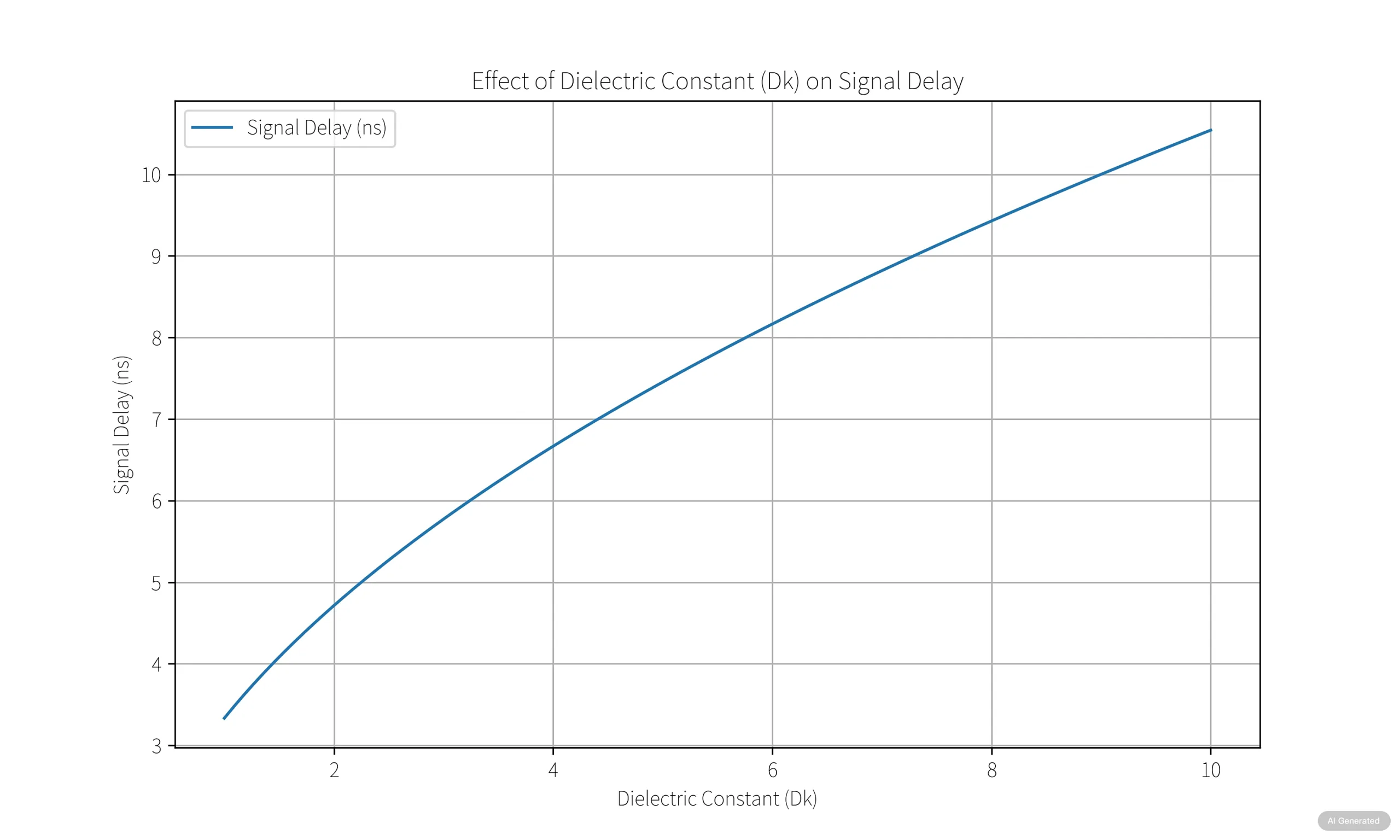
RF PCB Physics: Decoding Signal Integrity Equations
High-frequency circuit performance follows fundamental EM laws:
Signal Velocity Formula
v = c / √(Dk)
(c = light speed, Dk = dielectric constant)
Insertion Loss Model
IL = 4.34 × α × l
(α = attenuation coefficient, l = transmission length)
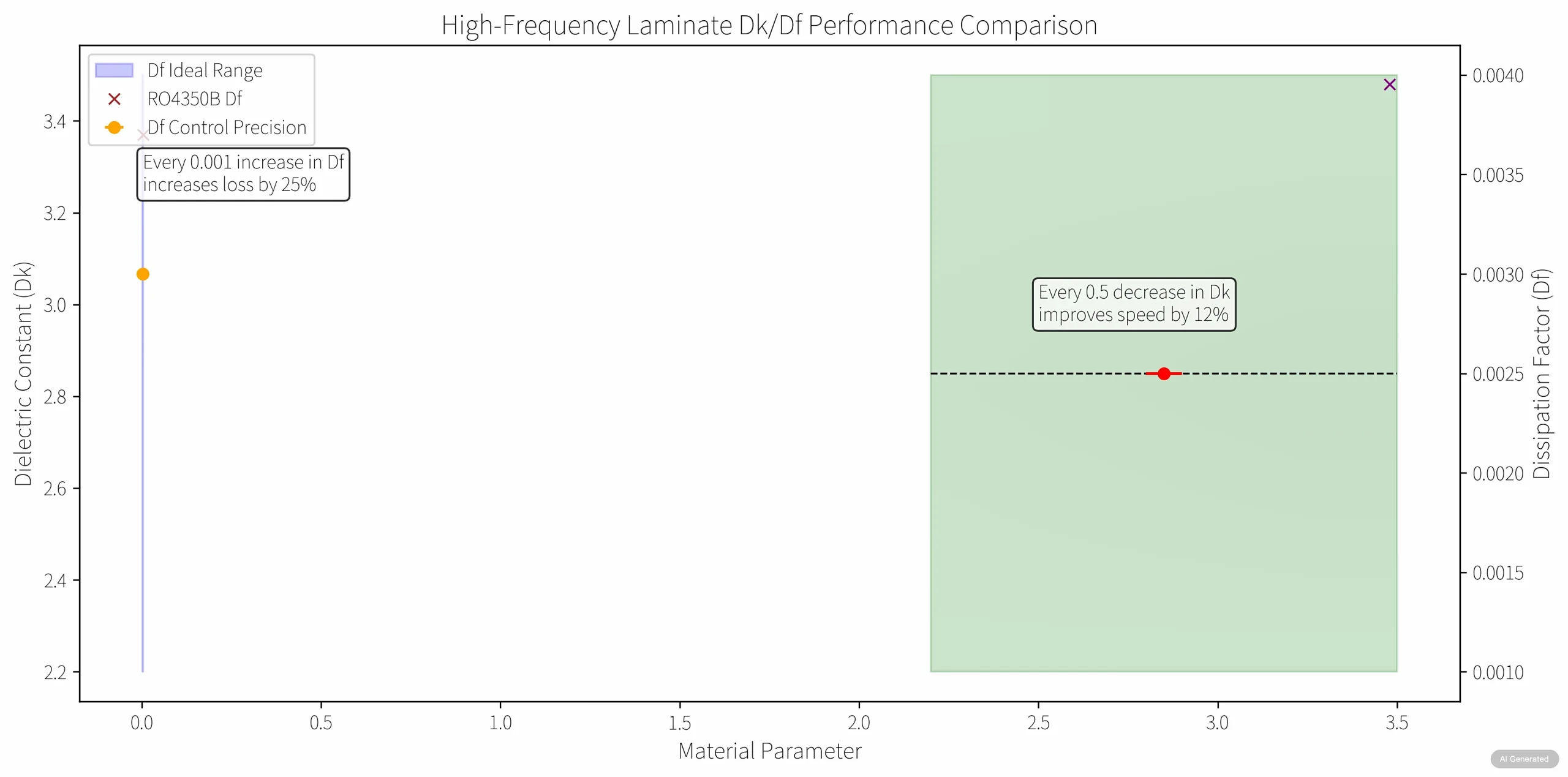
Precision Game in PCB Material Science
Critical Parameter Control Matrix
-
Non so: Ideal 2.2-3.5 | Speed ↑12% per 0.5 riduzione | UGPCB precision: ± 0,05
-
Df @10ghz: <0.004 | Loss ↑25% per 0.001 aumento | UGPCB: 0.003±0.0005
-
Assorbimento d'acqua: <0.2% | Df variation ≤8% @10% humidity | UGPCB: 0.18%
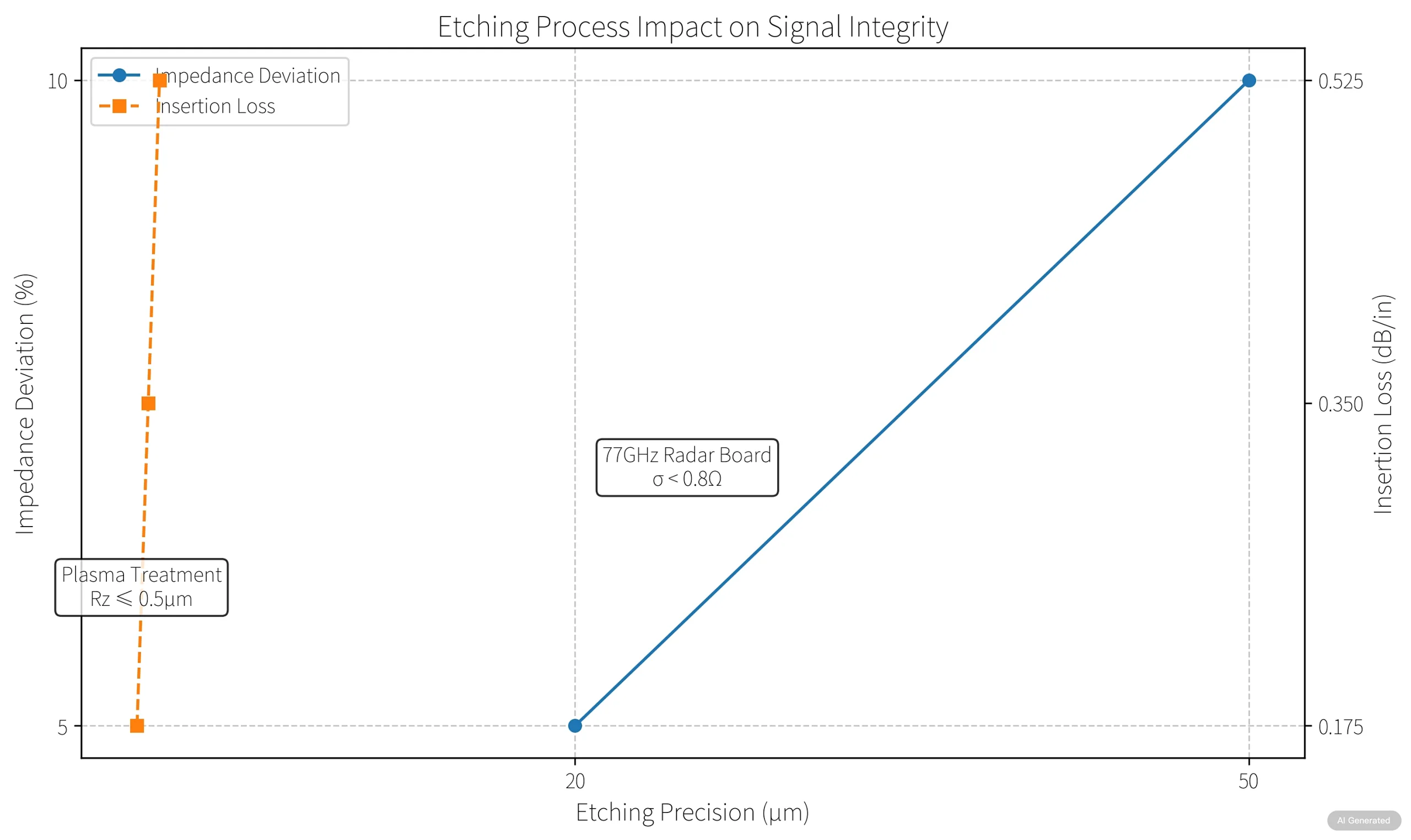
UGPCB’s Core Manufacturing Breakthroughs
Nanoscale Precision Control
-
Tolleranza: ±0.02mm (Industry standard: ± 0,05 mm)
-
Larghezza della linea: 3/3mil (76.2μm) ultra-fine lines
-
Controllo dell'impedenza: ±5% error (Industria: ±10% at high freq)
Caso di studio: 77GHz automotive radar board achieved σ<0.8Ω impedance consistency
Low-Loss Process Innovation
Proprietary “3-Step Etching Control”:
-
Plasma pretreatment (Surface roughness ≤0.5μm)
-
Dynamic etch compensation (Line width algorithm)
-
Nano-coating protection (Df retention: 99.2%)
Millimeter-Wave Solution Architecture
5G Base Station PCB Design Paradigm
-
Hybrid dielectric design for 28/39GHz bands
-
CTE matching: X/Y-axis <14ppm/° C.
-
Phase stability: ±2.5°/m @40GHz
Automotive Radar Tech Stack
Antenna Array → Power Divider Network → Beamforming System
│                │                     │
Dk=3.0±0.1      Df<0.0035            Dk uniformity Δ<0.03
Demonstrated Client Value
Performance Milestones:
-
Satellite comms client: Insertion loss ↓31% (4.2dB/m → 2.9dB/m)
-
5G infrastructure supplier: Power capacity ↑ to 3W/mm (Industria: 2.2W/mm)
Fig 4: UGPCB RF PCBA in 5G Base Station Integration
[Alt: 5G-basestation-RF-PCBA-integration-UGPCB-antenna-board-supplier]
Launch Your High-Frequency Innovation
*”When your design faces 40GHz+ challenges, ±0.02mm tolerance could be the last defense for signal integrity”*
— Dr. Zhou, UGPCB Chief RF Engineer
Invito all'azione:
✉️ Submit designs: saldi@ugpcb.com
📞 Urgent requests: +86-135-4412-8719
WeChat
Scansiona il codice QR con WeChat