
“Perché i chip si danneggiano quando li maneggio circuito normalmente?"Molti ingegneri si sentono confusi quando devono affrontare danni ai circuiti causati da scariche elettrostatiche (ESD). Infatti, il corpo umano può generare una tensione elettrostatica fino a decine di migliaia di volt, superando di gran lunga il limite di tolleranza della maggior parte dei componenti elettronici.
Anche la più precisa PCB (Circuiti stampati) possono essere vulnerabili alle scariche elettrostatiche. Un tocco accidentale può causare il fallimento immediato di chip per migliaia di dollari.
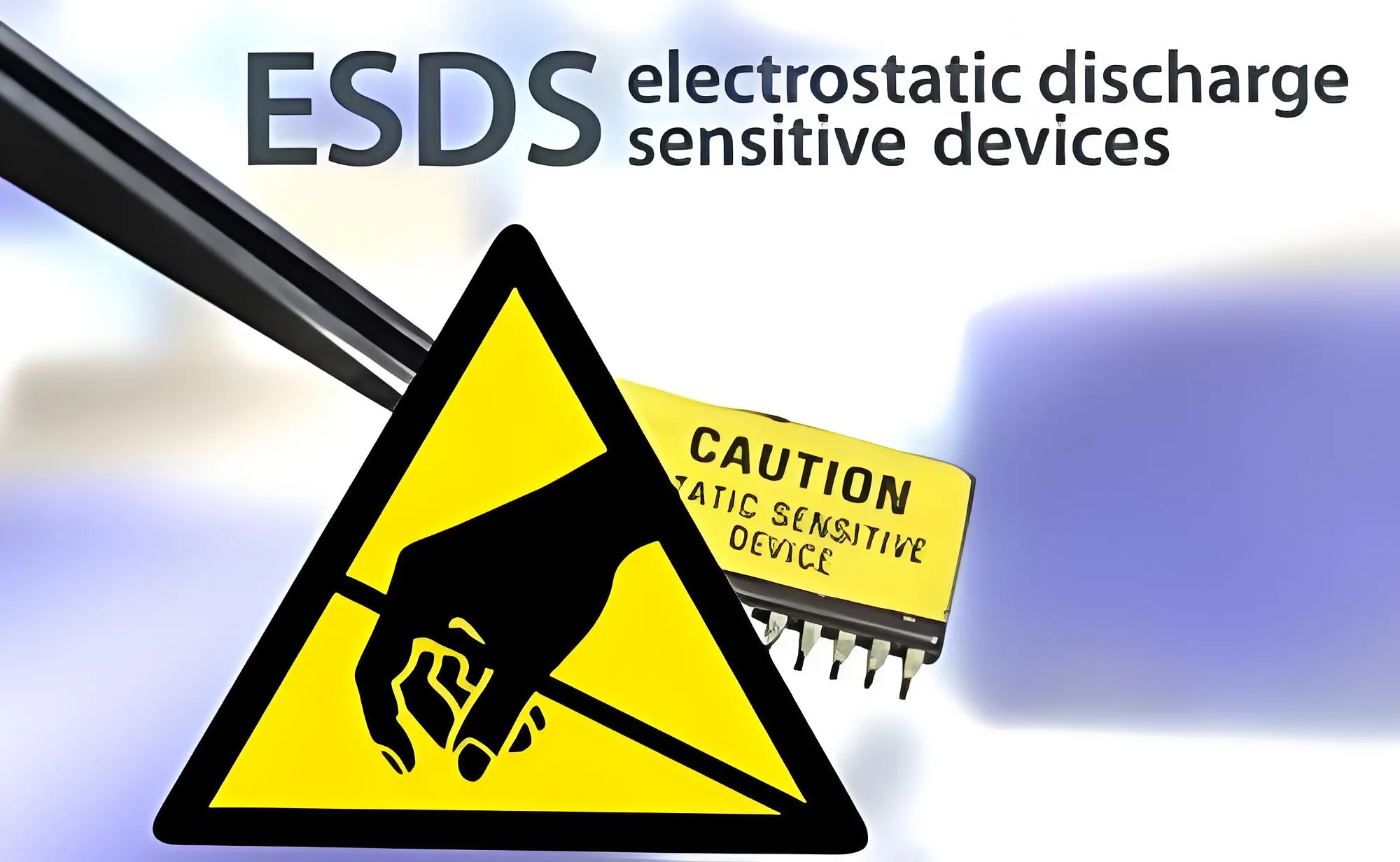
Sullo sfondo dei dispositivi elettronici sempre più sofisticati di oggi, La protezione ESD non è più una scelta facoltativa ma una misura necessaria per garantire l’affidabilità del prodotto. Questo articolo analizzerà in modo approfondito i punti chiave della progettazione e gli aspetti critici della produzione della protezione ESD del PCB, aiutando i tuoi prodotti a resistere a questo “fulmine invisibile”.
1. Minacce ESD: L'impatto letale dei fulmini invisibili in miniatura
L'ESD può essere immaginato come un fulmine invisibile in miniatura. Attività quotidiane come camminare, togliersi i maglioni, o anche prendere in mano una scatola di plastica può generare elettricità statica. La tensione di questa elettricità statica raggiunge spesso diverse migliaia di volt, o anche decine di migliaia di volt.
Il corpo umano stesso è in realtà il più grande generatore di elettricità statica. Soprattutto nelle stagioni secche, Le scariche elettrostatiche possono verificarsi nel momento in cui prendi in mano un PCB. Oggetti apparentemente insignificanti come i desktop di plastica, tappeti in fibra chimica, e le scatole per imballaggi in schiuma possono diventare “complici” dell’elettricità statica.
Le scariche elettrostatiche danneggiano i PCB in due forme principali:
- Danno grave: Questo è il danno più diretto ed evidente. L'ESD interromperà immediatamente i minuscoli circuiti all'interno del chip, causando danni permanenti al chip. Di conseguenza, il PCB smetterà di funzionare completamente, o funzioni specifiche (come porte seriali o ADC) fallirà direttamente.
- Danno cronico: Questo è più nascosto e problematico. L'ESD potrebbe non distruggere completamente il chip, ma può causare microdanni agli strati interni di ossido e ad altre strutture. Il PCB potrebbe funzionare ancora normalmente adesso, ma diventerà instabile e avrà una durata di servizio ridotta. Potrebbe improvvisamente non funzionare correttamente dopo alcuni giorni o a temperature specifiche. Questo errore intermittente è il più difficile da risolvere durante il debug e richiede molto tempo e impegno.
2. Diodi TVS: Il sistema di protezione contro i fulmini di precisione per i circuiti
TV (Soppressore di tensione transitoria) i diodi sono la prima linea di difesa contro le minacce ESD e i componenti di protezione più efficaci. Agiscono come "guardie di sicurezza per i segnali del circuito", mantenendo uno stato ad alta impedenza in condizioni normali. Una volta rilevato un impulso ESD, passano immediatamente a uno stato a bassa impedenza, deviando l'impulso ad alta tensione verso terra e proteggendo i chip backend.
2.1 Regole d'oro per il layout TVS
L'induttanza parassita è il più grande nemico delle prestazioni del TVS. L'induttanza parassita nel circuito, inclusa l'induttanza parassita degli stessi pin TVS, influisce sulla tensione di bloccaggio (Vc) sul circuito integrato di backend quando si verificano scariche elettrostatiche o picchi di tensione.
L'effetto protettivo di TVS segue la formula: VCL = VBR + RD × IPP. Tra loro:
- RD è la capacità parassita del TVS stesso; i prodotti con valori RD inferiori hanno una tensione di bloccaggio migliore e possono proteggere i circuiti integrati in modo più efficace.
- L'IPP è la corrente che attraversa il TVS durante l'istante di prova.
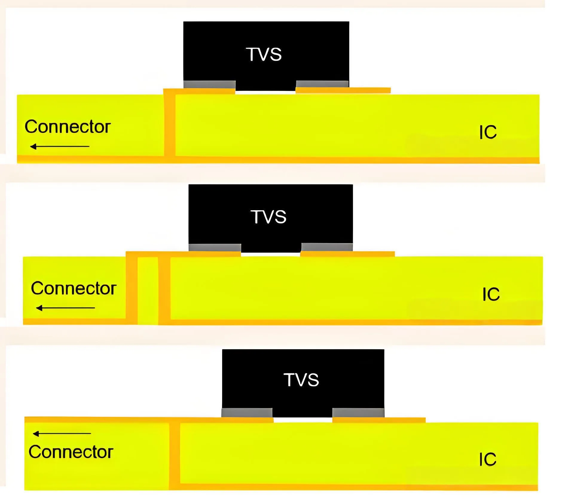
Per massimizzare l'effetto protettivo di TVS, è necessario assicurarsi che il collegamento a terra sia il più corto possibile e posizionare il TVS il più vicino possibile alla sorgente ESD. Ciò non solo riduce al minimo le EMI (Interferenza elettromagnetica) sul PCB ma riduce anche l'accoppiamento con altri percorsi. La scelta di un dispositivo TVS con un tempo di risposta inferiore a 1 ns fornisce una protezione ottimale per le interfacce ad alta velocità, fondamentali per PCBA (Gruppo a circuito stampato) affidabilità.
3. Layout e messa a terra del PCB: Le basi della protezione ESD
Ragionevole Disposizione del circuito stampato e la progettazione della messa a terra sono i pilastri della protezione ESD. Anche senza componenti di protezione aggiuntivi, possono migliorare significativamente l'immunità ESD del prodotto.
3.1 Punti chiave per il layout PCB
- Le linee del segnale ad alta velocità devono trovarsi a una distanza ≥ 3 mm dal bordo della scheda, mentre i segnali sensibili alle basse frequenze dovrebbero essere a ≥2 mm di distanza.
- I segnali critici come le linee dell'orologio e le linee di ripristino dovrebbero essere circondati da terra (schermatura del terreno). Disporre le linee di terra su entrambi i lati e aggiungere via di terra ogni 50 mm.
- Tutti gli involucri metallici esposti devono essere messi a terra a punto singolo tramite un resistore da 1 MΩ per evitare la formazione di un circuito a bassa impedenza attraverso la messa a terra diretta.
- È necessario mantenere una distanza superficiale ≥ 5 mm tra i componenti a contatto con l'utente (come pulsanti e manopole) e la scheda principale. Utilizzare schiuma conduttiva o molle metalliche per ottenere un collegamento equipotenziale.
- Impostare gli spinterometri (con una spaziatura di 0,2 mm–0,5 mm) nella posizione Pin1 del connettore e nel punto di messa a terra della custodia metallica. Queste misure possono guidare efficacemente la corrente ESD per scaricarla in modo sicuro ed evitare danni ai circuiti sensibili.
3.2 Principi per la progettazione della messa a terra di PCB
Quando si progetta un doppio strato o PCB multistrato, cercare di garantire un piano di massa completo e di ampia area. Un piano terra completo è come una vasta pianura: può assorbire e disperdere rapidamente l'energia ESD, impedendo l'accumulo di energia in un singolo punto. Allo stesso tempo, fornisce un percorso di scarica efficiente per i diodi TVS.
Durante il layout del PCB, riempire la rete di terra con rame e assicurarsi che il rame di terra copra gran parte dell'area vuota sulla scheda (senza tracce) possibile. Per tutte le interfacce esterne (come porte USB e prese di alimentazione CC), collegare l'involucro metallico alla terra della scheda tramite un condensatore ad alta tensione o direttamente. Da questa parte, Le scariche elettrostatiche verranno deviate attraverso l'involucro prima di entrare nel circuito, migliorando la protezione ESD del PCB a livello di interfaccia.
4. Processo di laminazione: La barriera di protezione interna per PCB multistrato
Nei PCB multistrato, la qualità del processo di laminazione è direttamente correlata alla capacità di protezione ESD interna del pannello. Se il dielettrico tra due strati conduttori è troppo sottile, le scariche elettrostatiche ad alta tensione possono facilmente danneggiarlo, provocando danni permanenti.
4.1 Ruolo principale del prepreg
Pre -preg (materiale composito preimpregnato) funge da dielettrico isolante interstrato nei PCB multistrato. È un “materiale composito funzionale” controllato da processi di produzione di precisione, la sua caratteristica principale è che la resina è in uno "stato semi-indurito di fase B", una caratteristica fondamentale per realizzare la laminazione di schede multistrato.
Il prepreg non solo fornisce un legame fisico ma ottiene anche tre effetti: isolamento elettrico + supporto strutturale. Le sue prestazioni di isolamento e le proprietà dielettriche determinano direttamente l'affidabilità elettrica del PCB: dopo la polimerizzazione, la resistività del volume è ≥10¹⁴Ω·cm, e la resistenza alla tensione di rottura è ≥20kV/mm, che può bloccare le perdite dell'interstrato, fondamentali per prevenire danni all'interstrato indotti dalle scariche elettrostatiche.
I parametri principali di Prepreg includono:
- Contenuto di resina (RC%): Normalmente 50%~70%, che determina la forza del legame interstrato e lo spessore dello strato dielettrico.
- Fluidità: 15~30 mm.
- Temperatura di transizione vetrosa (Tg): Normalmente 150~200℃.
- Costante dielettrica (Non so): 4.2±0,2 per il normale FR-4 Prepreg.
4.2 Controllo di qualità per il processo di laminazione
Per garantire la qualità della laminazione, il coefficiente di dilatazione termica (Cte) di Prepreg deve corrispondere a quello dei pannelli centrali FR-4 e dei fogli di rame. Se la deviazione CTE dell'asse Z supera 5 ppm/℃, È probabile che si verifichino rotture tra gli strati durante i cicli di temperatura.
Durante la laminazione:
- Quando la temperatura dello strato intermedio è 80~130℃, la differenza di temperatura tra lo strato superiore della piastra portante e lo strato intermedio non deve superare i 25 ℃, e la velocità di riscaldamento non deve superare 1,3~5℃/min.
- Quando la temperatura raggiunge 85±5℃, determinare il tempo necessario per passare dalla bassa pressione alla media pressione.
- Quando la temperatura raggiunge 110±5℃, determinare il tempo necessario per passare dalla pressione media all'alta pressione.
Nella moderna produzione di PCB, la tecnologia della pressa a vuoto ha migliorato significativamente la qualità della laminazione. L'ambiente sottovuoto evita la formazione di bolle e vuoti, garantire un flusso e un riempimento uniformi della resina Prepreg, rafforzando la resistenza del PCB multistrato alla rottura da scariche elettrostatiche.
5. Processi avanzati e verifica della qualità
Man mano che i dispositivi elettronici si sviluppano verso l'alta frequenza e l'alta densità, La protezione ESD deve affrontare nuove sfide e richiede soluzioni di processo più avanzate.
5.1 Miglioramenti dei processi per applicazioni speciali
- Scenari di comunicazione ad alta frequenza: Preimpregnato a basso Dk (Dk=3,48±0,03, Df<0,004) può soddisfare i requisiti di trasmissione del segnale a 28 GHz/77 GHz fornendo allo stesso tempo una protezione di isolamento affidabile, fondamentale per mantenere l'integrità del segnale e la resistenza ESD nei PCB 5G o radar automobilistici.
- Tavole di rame spesse (≥3 once): Adottare la "laminazione Prepreg a doppio strato a basso contenuto di resina" (52%±1% per strato, contenuto totale di resina 56%) combinato con laminazione ad alta pressione da 8 MPa. Ciò può aumentare la resistenza alla tensione di rottura dello strato dielettrico fino a 3.500 V, migliorando la protezione ESD per i PCB legati all'alimentazione.
- ISU (Interconnessione ad alta densità) assi: Richiede preimpregnato a bassa fluidità (18±2mm) + laminazione sotto vuoto per risolvere il problema del trabocco della resina microvia da 0,075 mm. Questi speciali trattamenti di processo non solo migliorano le prestazioni del prodotto, ma migliorano anche la capacità di protezione ESD interna del circuito.
5.2 Standard di verifica e test di qualità
Un sistema di verifica della qualità a circuito chiuso è fondamentale per garantire le capacità di protezione ESD del PCB. Include:
- Ispezione in arrivo: Utilizzare spettrometri a infrarossi per testare il contenuto volatile e spettrometri dielettrici per verificare la stabilità Dk/Df.
- Monitoraggio del processo: Raccogli i dati di temperatura e pressione in tempo reale durante la laminazione.
- Verifica del prodotto finito: Eseguire test di resistenza alla pelatura dell'interstrato e test di resistenza all'isolamento.
La verifica finale della protezione ESD deve soddisfare i requisiti Livello IEC61000-4-2 4 standard, i.e., test di scarica a contatto fino a ±8 kV e scarica in aria fino a ±15 kV. Dopo il test, devono essere soddisfatti i seguenti criteri:
- Integrità del segnale (apertura del diagramma oculare >70%).
- Tasso di errore sui bit (<1×10^-12).
- Fluttuazione della corrente operativa (<± 5%).
- Azzerare i tempi (0 tempi/ciclo di prova).
 Gli odierni processi di produzione dei chip stanno diventando sempre più sofisticati, ma ciò non significa che possiamo abbassare la nostra vigilanza contro l’ESD. Al contrario, man mano che le dimensioni del circuito si riducono e le tensioni operative diminuiscono, i componenti diventano più sensibili alle scariche elettrostatiche.
Gli eccellenti ingegneri PCB prendono in considerazione la protezione ESD nella fase iniziale della progettazione, integrare misure di protezione nel “DNA” del prodotto. Questa non è solo una sfida tecnica, ma anche una prova di responsabilità e professionalità, perché la migliore riparazione dei guasti è innanzitutto prevenire che si verifichino..
