Professional Product Overview
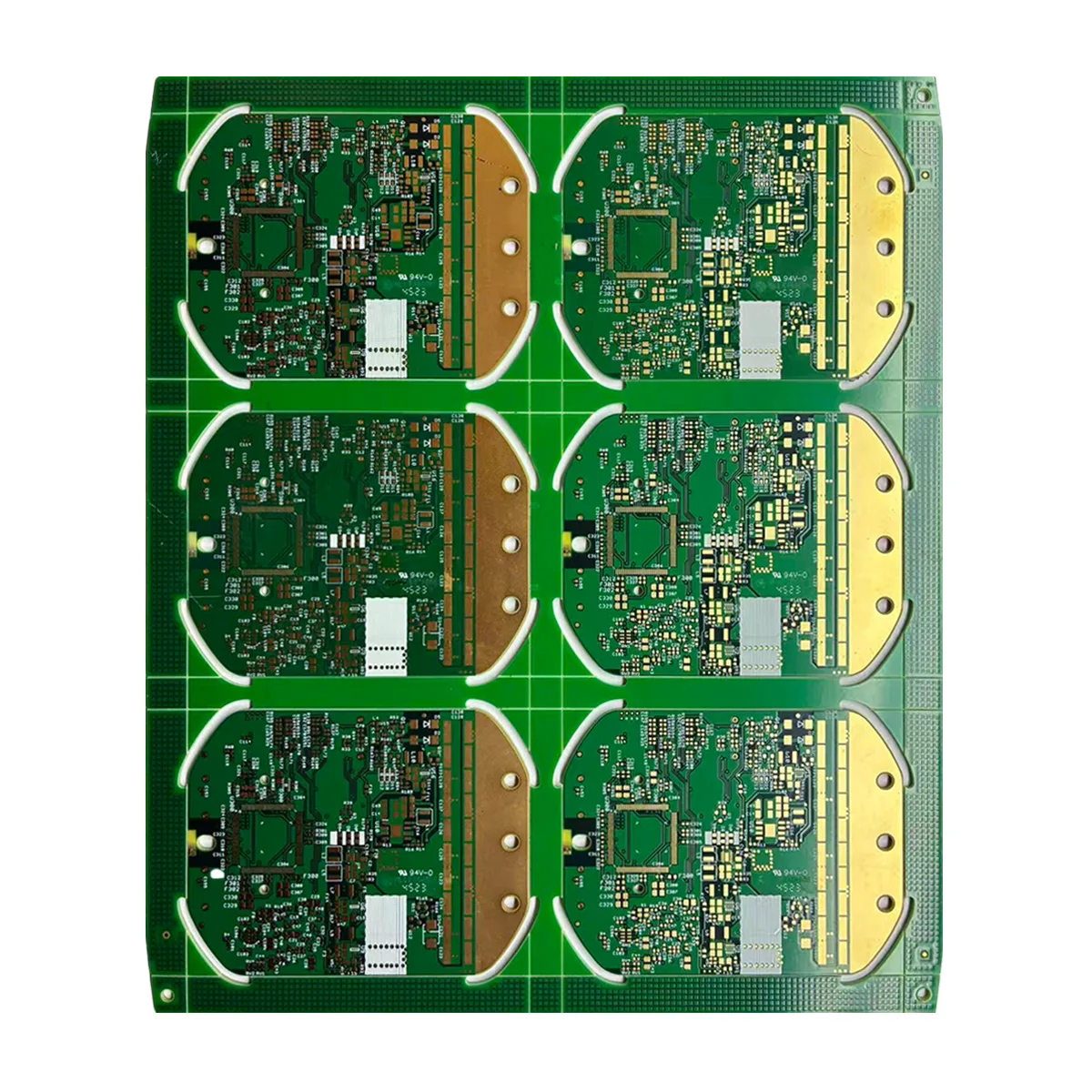
The UGPCB 12-Layer Rigid PCB is a high-end circuito multistrato engineered for complex signal transmission, high-density interconnects (ISU), and demanding operating environments. Manufactured with high-performance FR-4 TU872SLK laminate and finished with 2-microinch Immersion Gold (Essere d'accordo), this board is a cornerstone solution for industrial control systems, infrastrutture di telecomunicazioni, and advanced computing hardware, offering exceptional electrical performance, long-term reliability, and robust signal integrity.

Definizione del prodotto & Classificazione
This product is classified as a High-Layer Count Rigid Printed Circuit Board. It can be further categorized as:
-
By Structure: Rigid PCB.
-
Per conteggio strati: 12-Layer Multilayer Board (mid-to-high layer count).
-
Per tecnologia: Standard Multilayer PCB suitable for complex, non-extreme miniaturization designs.
-
By Application Class: Industrial/Telecom-Grade PCB, meeting requirements for high reliability and long-term stability.
Considerazioni critiche sulla progettazione
Designing a 12-layer PCB requires meticulous attention to:
-
Stack-up Design: A rational stack-up sequence (per esempio., alternating signal-ground-signal layers) is paramount for impedance control, crosstalk reduction, and Electromagnetic Compatibility (EMC). A proper 12-layer stack-up provides excellent power integrity and signal shielding.
-
Controllo dell'impedenza: For high-speed digital signals (per esempio., DDR, PCIe) or RF lines, precise calculation and control of trace characteristic impedance (per esempio., 50Ω single-ended, 90Differenziale Ω/100Ω) are essential. We utilize advanced EDA tools and precise process controls to ensure consistency.
-
Energia & Ground Plane Management: Solid ground planes and optimized power segmentation ensure low-noise power delivery and clear return paths, which are critical for system stability.
-
Gestione termica: The 1.6mm board thickness and the thermal properties of FR-4 must align with component power dissipation. High-power areas may require thermal vias or integration with external cooling solutions.
Come funziona
A PCB is a passive platform that provides mechanical support, electrical interconnection, and signal transmission pathways for electronic components. This 12-layer PCB facilitates a complete working system by connecting chips, resistori, condensatori, ecc., through a complex network of etched copper traces. The multilayer architecture allows traces to cross on different layers without interference, significantly increasing circuit complexity and integration density. The ENIG surface finish guarantees reliable solder joints and long-term contact stability.
*(Suggerimento di immagini: Detailed cross-sectional diagram of a 12-layer PCB stack-up)*
*Testo alternativo: Cross-sectional view of a 12-layer PCB stack-up showing alternating copper layers and dielectric, illustrating complex internal structure for high-density interconnect.*
Costruzione & Materiali
-
Layer Structure: 12 conductive copper layers laminated with insulating prepreg.
-
Materiale principale: FR-4 TU872SLK. This is a high-performance epoxy glass laminate offering advantages over standard FR-4:
-
Higher Thermal Stability (Alto tg, typically ≥170°C), providing better resistance to thermal expansion.
-
Superior Electrical Properties, with stable Dielectric Constant (Non so) e fattore di dissipazione (Df) under high-temperature and high-frequency conditions.
-
Excellent CAF (Conductive Anodic Filament) Resistance, ideal for high-voltage, high-humidity environments, ensuring superior reliability.
-
-
Spessore finito: 1.60mm (nominal), with tight tolerance control (tipicamente ±10%).
-
Finitura superficiale: Oro per immersione in nichel chimico (Essere d'accordo). Nickel thickness: 3-5μm; Spessore dell'oro: 2 microinches (ca. 0.05μm). The gold layer protects the nickel from oxidation, providing a flat, superficie saldabile, while the nickel acts as a diffusion barrier between copper and gold.
Caratteristiche chiave & Prestazione
-
Alta affidabilità: TU872SLK high-Tg material and ENIG finish ensure resistance to high temperatures, corrosion, and suitability for long-term operation in harsh environments.
-
Ottima integrità del segnale: Rigorous stack-up design and impedance control guarantee high-speed signal quality and lower bit error rates.
-
Strong Load-Bearing & Thermal Capacity: The 1.6mm thickness offers robust mechanical strength and substantial thermal load management.
-
Precision Solder Platform: The flat 2μ” ENIG surface is ideal for fine-pitch componenti (per esempio., Bgas), resulting in strong, reliable solder joints with low defect rates.
-
Interconnessione ad alta densità (ISU): Twelve routing layers support complex, dense circuit designs, enabling reduced product footprint.
Manufacturing Process Flow
Inner Layer Imaging → AOI Inspection → Lamination & Pressing → Drilling → Electroless Copper Deposition → Outer Layer Imaging → Pattern Plating → Etching → Solder Mask Application → ENIG Surface Finish → Routing & Profiling → Electrical Testing → Final Quality Control (FQC)
Applicazioni & Casi d'uso
This PCB is widely used in stability and performance-critical fields:
-
Automazione industriale: PLC controllers, servo drives, industrial robot control boards.
-
Telecommunications Equipment: Router, interruttori, base station cards, optical modules.
-
Elettronica medica: Control units for advanced medical imaging systems, patient monitors.
-
Test & Strumenti di misura: High-precision oscilloscopes, analizzatori di spettro, signal generators.
-
Energia & Energy: Inverter control boards, Sistema di gestione della batteria (BMS) assi, smart meters.
-
Elettronica automobilistica: High-end infotainment systems, Sistemi avanzati di assistenza alla guida (Adas) domain controllers.