

Panoramica del prodotto
Il PCB HDI 8L con foro svasato 2+N+2 di UGPCB con foro cieco è un PCB ad alte prestazioni circuito stampato progettato per applicazioni elettroniche avanzate. Questo PCB integra l'interconnessione ad alta densità (ISU) tecnologia con fori svasati e vie cieche, offrendo affidabilità superiore per prodotti digitali intelligenti. Con una struttura a 8 strati, supporta progetti complessi pur mantenendo un fattore di forma compatto, rendendolo ideale per dispositivi con vincoli di spazio. I parametri chiave includono uno spessore finito di 1,0 mm, Materiale FR-4, e trattamento superficiale con oro ad immersione, garantendo durata ed efficiente trasmissione del segnale.
Definizione del prodotto
Questo PCB è definito come una scheda HDI a 8 strati con una struttura di accumulo 2+N+2, che si riferisce a due cicli di laminazione sequenziali con uno strato centrale (N). Incorpora fori svasati (incavi conici per le teste delle viti) e passaggi ciechi che collegano gli strati esterni agli strati interni senza penetrare nell'intera scheda. Questo design migliora la densità di instradamento e riduce le dimensioni, catering per il moderno Progettazione di circuiti stampati tendenze per le applicazioni ad alta velocità.
Punti chiave della progettazione
Durante la progettazione di questo PCB, i fattori critici includono la riduzione al minimo di traccia e spazio a 3mil/3mil per il routing ad alta densità, e rispettando le specifiche relative alle dimensioni del foro: fori meccanici da 0,2 mm e fori ciechi realizzati al laser da 0,1 mm. Lo spessore del rame (interno 1 OZ, esterno 0,5 OZ) deve bilanciare la capacità di carico di corrente e l'integrità del segnale. I progettisti dovrebbero dare priorità alla gestione termica e al controllo dell'impedenza, soprattutto per assemblaggio PCBA processi, per evitare problemi come la perdita di segnale. Si consiglia di utilizzare il software di progettazione PCB HDI per ottimizzare l'impilamento dei livelli e il posizionamento.
Principio di lavoro
Il PCB funziona facilitando le connessioni elettriche tra i componenti attraverso la sua struttura a strati. I fori ciechi consentono le interconnessioni tra strati specifici, riducendo la lunghezza del percorso del segnale e migliorando la velocità, mentre i fori svasati forniscono stabilità meccanica per il montaggio dei componenti. IL ISU la tecnologia consente percorsi più brevi, migliorare le prestazioni nelle applicazioni ad alta frequenza, come quelli trovati in PCB per dispositivi intelligenti.
Applicazioni e usi

Questo PCB è ampiamente utilizzato nei prodotti digitali intelligenti, compresi gli smartphone, compresse, dispositivi indossabili, e apparecchiature IoT. Il suo design ad alta densità supporta funzionalità avanzate come la connettività 5G e l'elaborazione AI, rendendolo la scelta migliore per i produttori di PCB focalizzati sull'innovazione. Le applicazioni si estendono all'elettronica automobilistica e ai dispositivi medici dove l'affidabilità è fondamentale.
Classificazione
Basato sulla struttura, questo prodotto rientra nel PCB HDI categoria, nello specifico una tipologia 2+N+2 con via cieca ed interrata. Può essere classificato in base al numero di strati (8L), materiale (FR-4), e finitura superficiale (oro di immersione + OSP), allineandosi agli standard del settore per soluzioni PCBA di fascia alta.
Materiali utilizzati
Il materiale primario è FR-4, un laminato epossidico ignifugo noto per il suo eccellente isolamento elettrico e resistenza meccanica. Lamine di rame (1Interno OZ, 0.5Esterno OZ) fornire conduttività, mentre il trattamento superficiale in oro per immersione offre resistenza alla corrosione e saldabilità, cruciale per l'assemblaggio PCBA. Questa selezione di materiali garantisce che il PCB soddisfi la conformità RoHS per la sicurezza ambientale.
Caratteristiche delle prestazioni
I punti salienti delle prestazioni includono un'elevata stabilità termica, bassa perdita di segnale, e controllo dell'impedenza. Con una larghezza minima della traccia di 3mil, supporta la trasmissione dati ad alta velocità. La tecnologia del foro cieco riduce la capacità parassita, migliorare l'integrità del segnale. Queste caratteristiche lo rendono affidabile per applicazioni PCB impegnative, come nei prodotti digitali ad alta frequenza.
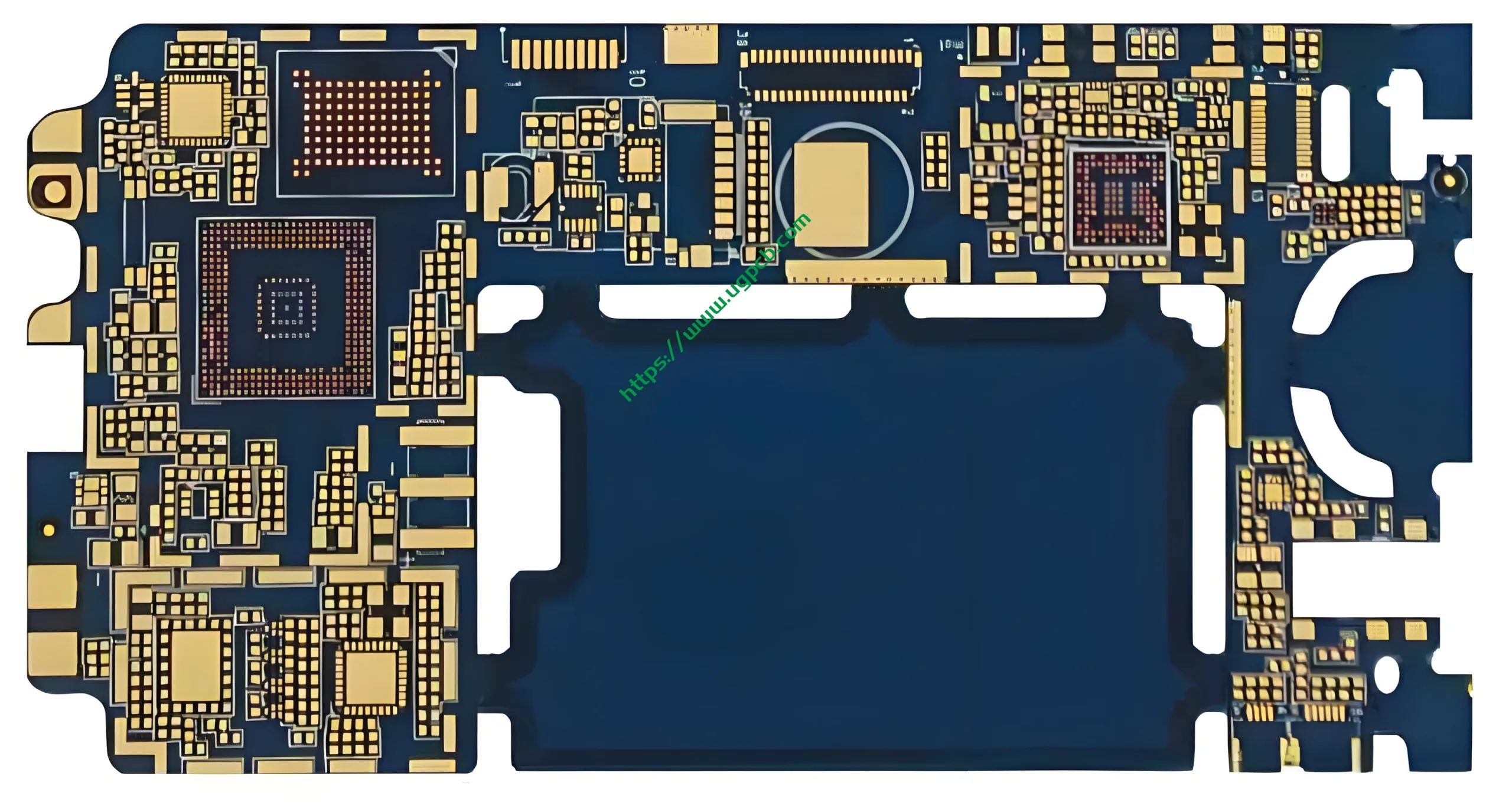
Dettagli strutturali
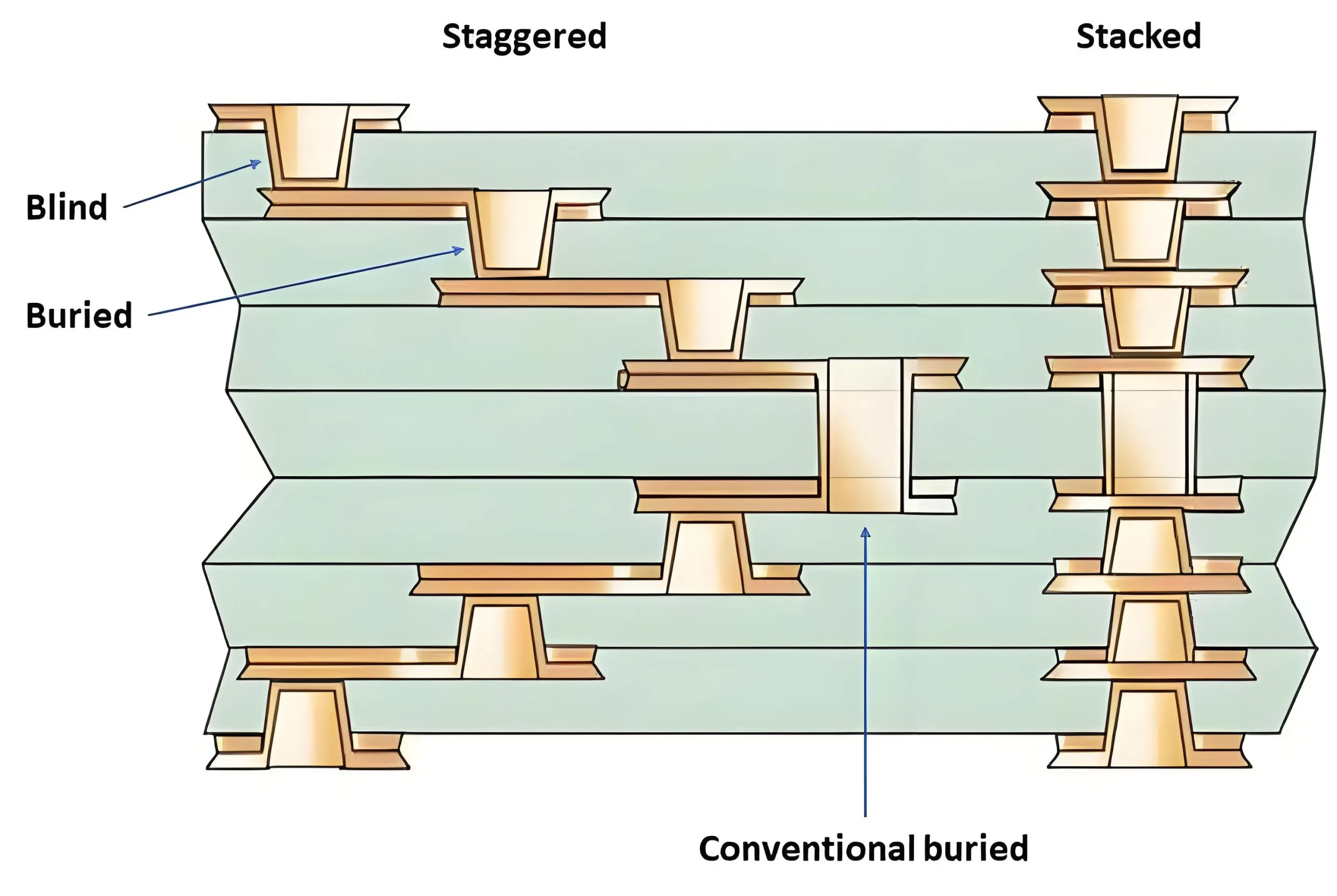
La struttura è composta da 8 strati con una costruzione simmetrica: due strati esterni collegati tramite vie cieche agli strati interni, che circonda un nucleo. I fori svasati sono realizzati sulla superficie per un montaggio sicuro dei componenti. Questo layout massimizza l'efficienza dello spazio e supporta progetti PCBA complessi, come quelli con Componenti BGA.
Caratteristiche chiave
Le caratteristiche principali includono funzionalità di miniaturizzazione, maggiore affidabilità grazie alle robuste strutture via, e compatibilità con la saldatura senza piombo. La maschera di saldatura blu o bianca facilita l'ispezione, mentre lo spessore di 1,0 mm garantisce durata. Questi attributi lo rendono la scelta preferita per l'approvvigionamento di PCB nell'elettronica all'avanguardia.
Processo di produzione
Il processo di produzione comprende più fasi: imaging dello strato interno, laminazione, foratura laser di vie cieche, perforazione meccanica di fori svasati, placcatura, e finitura superficiale. La garanzia della qualità prevede test elettrici e ispezione ottica automatizzata (AOI) per garantire il rispetto delle specifiche. Questo flusso di lavoro enfatizza la precisione Produzione PCB HDI, garantendo un'elevata resa produttiva per la successiva integrazione PCBA.
Scenari di utilizzo
Gli scenari di utilizzo comuni includono l'elettronica di consumo come i dispositivi domestici intelligenti, sistemi di automazione industriale, e hardware di comunicazione. È ideale per applicazioni che richiedono dimensioni compatte, PCB ad alta velocità, come nel PCBA per sistemi embedded o unità di controllo automobilistiche. Questa versatilità supporta l'innovazione nelle tecnologie basate su PCB.


