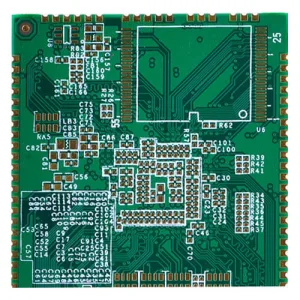
What is High-Speed Board Design?
High-speed design specifically refers to systems that use high-speed digital signals to transfer data between components. The line between high-speed digital designs and simple circuit boards with slower digital protocols is blurred. A common metric used to denote a particular system as “ad alta velocità” is the edge rate (or rise time) of the digital signals used in the system. Most digital designs use both high-speed (fast edge rate) and low-speed (slow edge rate) digital protocols. In today’s era of embedded computing and the Internet of Things, most high-speed circuit boards have an RF front-end for wireless communication and networking.
Considerations for PCB Stack-Up in High-Speed Signal Design
All PCB stack-ups include a set of layers dedicated to high-speed signal, energia, and ground planes, and the following points need to be considered when assigning layers in the stack-up:
Board Size and Net Count
- How big is the board and how many nets need to be routed in the PCB layout? A physically larger board may have enough space for you to route the entire PCB layout without using multiple signal layers.
Routing Density
- With a high number of nets and board size constrained by a small area, you may not have enough room to route around the surface layers. So when the traces are closer together, you will need more internal signal layers. Using a smaller board size can force higher routing density.
Number of Interfaces
- Sometimes routing only one or two interfaces per layer is a good strategy, depending on the width of the bus (serial vs. parallel) and board size. Keeping all signals in a high-speed digital interface on the same layer ensures that all signals see consistent impedance and skew.
Low-Speed and RF Signals
- Will there be low-speed digital or RF signals in your digital design? If so, these may take up surface space available for high-speed buses or components, and may require additional internal layers.
Integrità del potere
- One of the cornerstones of power integrity is the use of large power and ground planes for every voltage level required by a large IC. These should be placed on adjacent layers to help ensure that there is high plane capacitance to support a stable power supply with decoupling capacitors.
 LOGO UGPCB
