Copper-Based Printed Circuit Board Material Composition
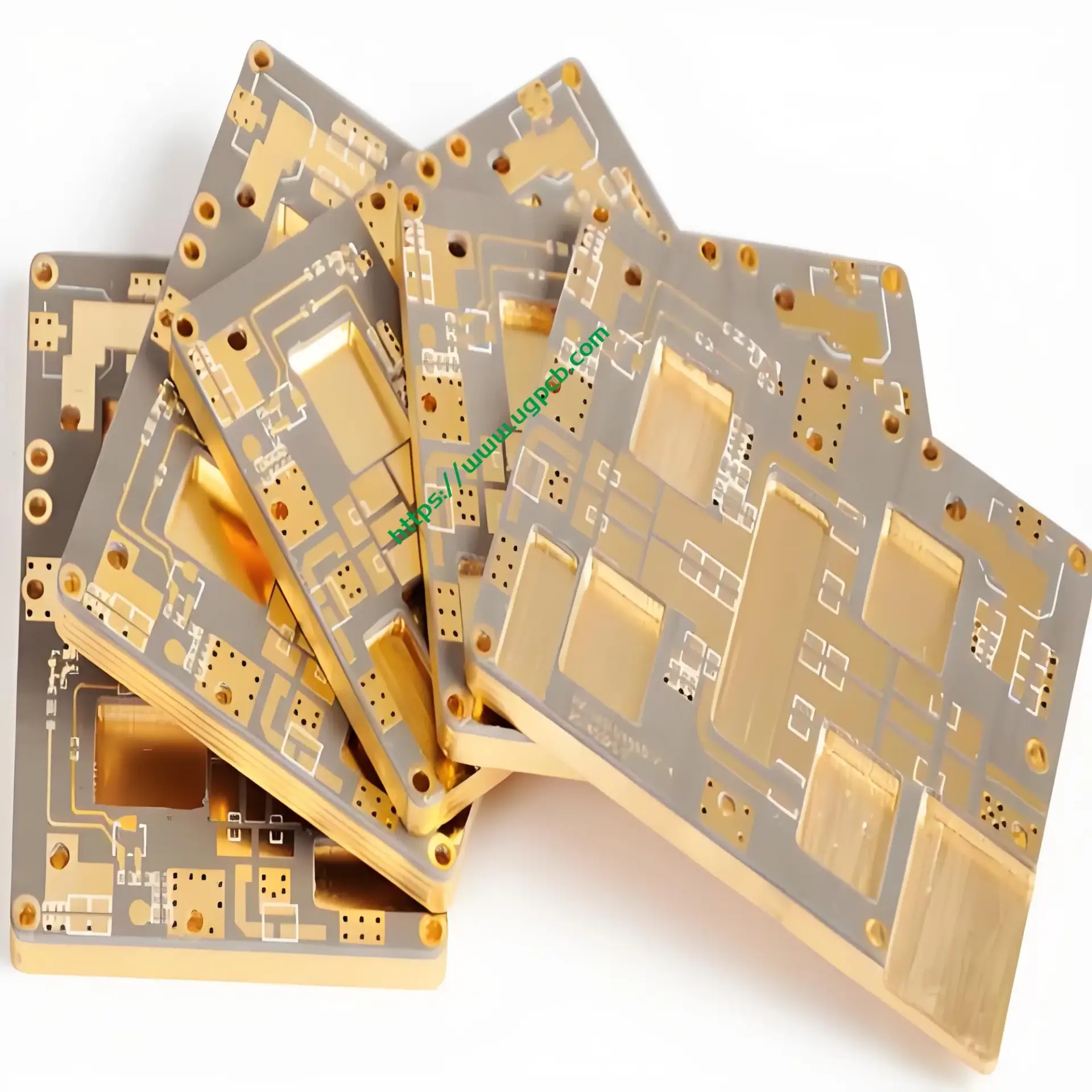
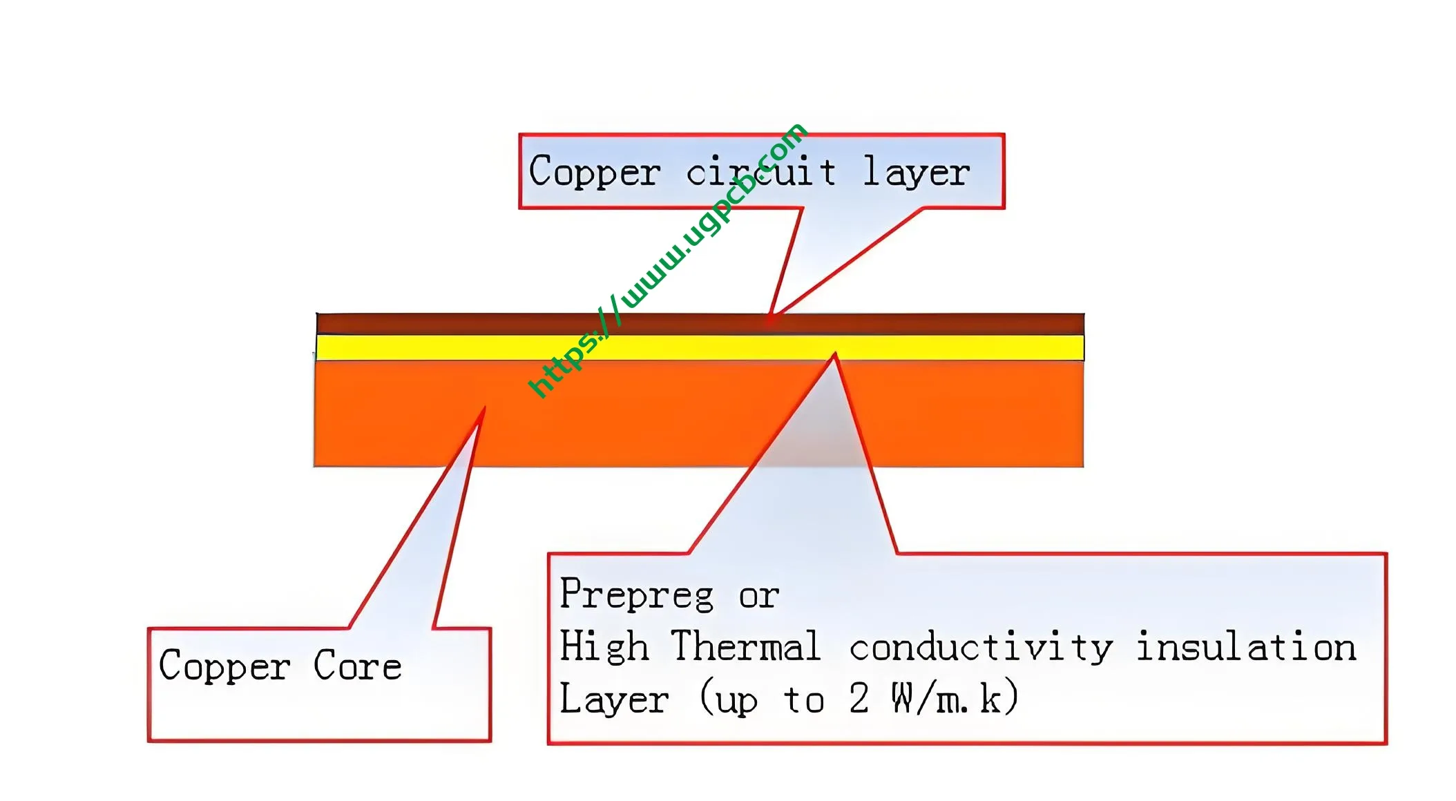
The Copper-Based Printed Circuit Board (PCB) is primarily composed of a copper base, which provides excellent conductivity and thermal stability. This model features a single layer design, making it suitable for a range of applications requiring efficient electrical pathways.
Performance Capabilities
With a finished thickness of 4.0mm and a copper thickness of 3OZ, Questo PCB is robust and capable of handling high currents and temperatures. The copper base ensures superior heat dissipation, crucial for maintaining performance in demanding environments.
Distinctive Characteristics
Disponibile in verde o bianco, this PCB stands out with its Osp (Conservante organico di saldabilità) Trattamento superficiale, which protects the copper circuitry from tarnishing and ensures reliable soldering. Inoltre, it features a special process known as step hole PCB, allowing for multi-level interconnection, ideal for complex circuit designs.
Flusso di lavoro di produzione
The production of this copper-based PCB begins with the preparation of the copper base material. Prossimo, the circuitry is etched onto the copper layer using advanced photolithographic techniques. After etching, the Osp treatment is applied to preserve the copper’s solderability. The PCB is then inspected for quality and undergoes drilling for step holes, a process that enables vertical electrical connections across different layers. Finalmente, the PCB is cut to size and prepared for shipping.

Scenari di applicazione
Due to its high performance and reliability, the Copper-Based Circuito stampato is ideal for high-end communication power supply applications. It is particularly suited for use in systems requiring high current handling, robust thermal management, and intricate circuit designs. Its ability to support step hole interconnectivity makes it an excellent choice for multi-layered and complex PCBs in telecommunication and power supply units.