
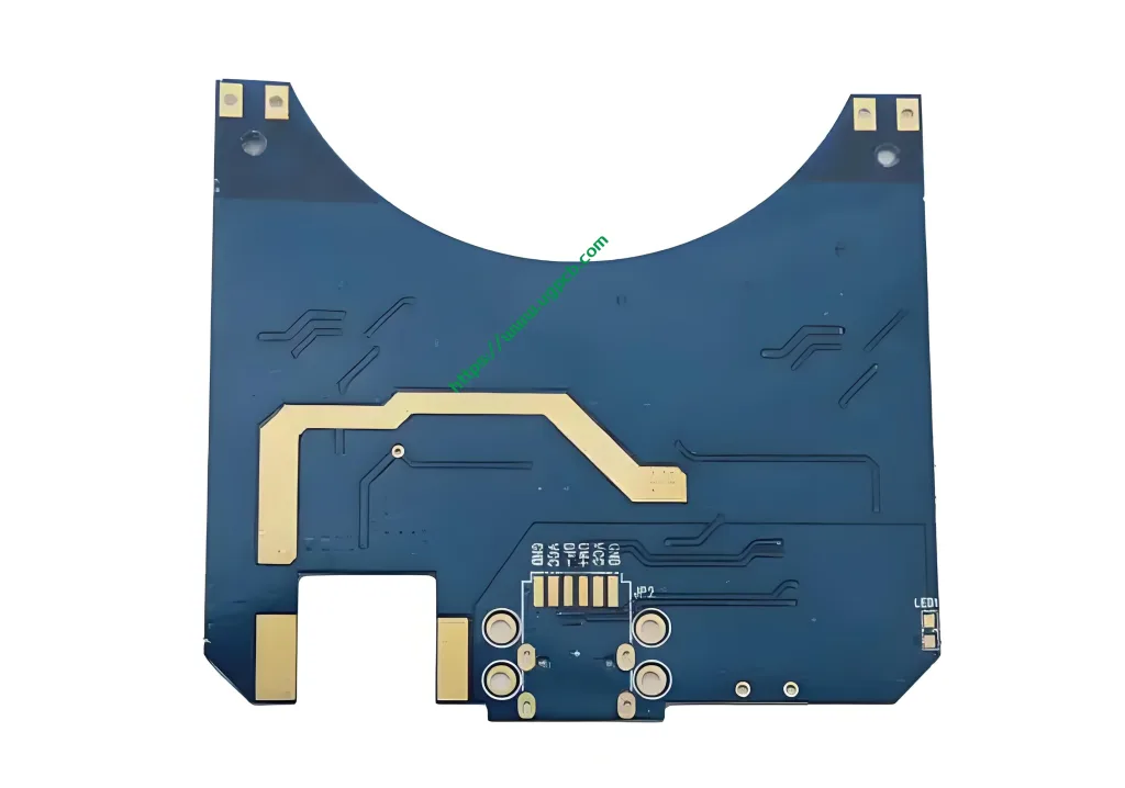

Composizione materiale
The Dark Blue 2 Layer PCB is constructed using high-quality FR4 (Ritardante di fiamma 4) materiale. FR4 is known for its excellent electrical properties, resistenza meccanica, e resistenza al calore, making it ideal for a wide range of applications.
Specifiche
This PCB features a sleek dark blue color with white silkscreen for a professional appearance. It has a finished thickness of 1.2mm, ensuring durability and stability. Lo spessore del rame è 1 oz, providing sufficient conductivity for electrical signals. Il trattamento superficiale è oro immersione, which enhances corrosion resistance and improves solderability.
Caratteristiche delle prestazioni
With a minimum trace width and spacing of 4mil (0.1mm), the Dark Blue 2 Layer PCB supports high-density circuit layouts. This makes it suitable for complex electronic designs that require precise and reliable connections. The immersion gold finish further enhances its performance by providing a protective layer that prevents oxidation and ensures long-term reliability.
Processo di produzione
The production of Dark Blue 2 Layer PCBs involves several steps:
- Progettazione e impaginazione: The PCB design is created using specialized software and then reviewed for accuracy.
- Preparazione del materiale: FR4 sheets of the required thickness are cut to size.
- Copper Lamination: A layer of copper is applied to both sides of the FR4 sheet.
- Incisione: The unwanted copper is removed to create the circuit pattern.
- Perforazione: Holes are drilled for components and interconnections.
- Placcatura: The holes are plated with copper to ensure electrical conductivity.
- Trattamento superficiale: An immersion gold finish is applied to protect the copper surfaces.
- Silkscreen Printing: Component labels and other markings are printed on the PCB.
- Assembly and Testing: Components are assembled, and the PCB is tested to ensure functionality.

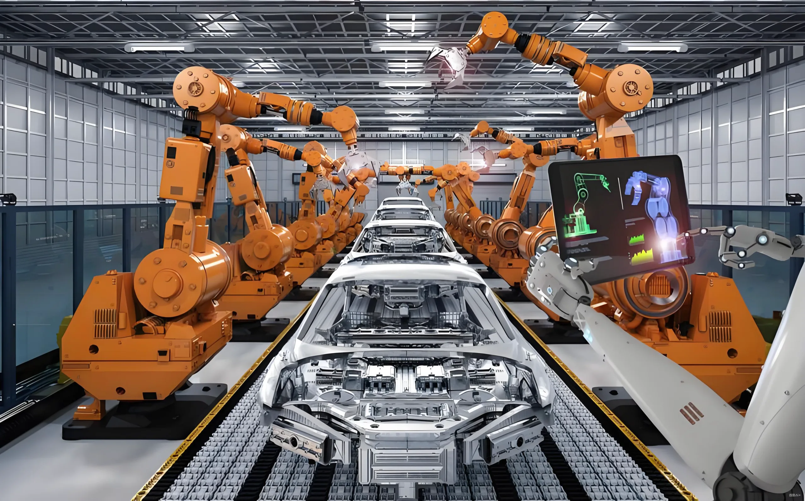
Scenari di applicazione
The Dark Blue 2 Layer PCB is ideal for a variety of digital applications, tra cui:
- Elettronica di consumo: Such as smartphones, compresse, and wearable devices.
- Computer Hardware: Including motherboards, schede grafiche, and other computer components.
- Controlli industriali: For automation systems, sensori, and other industrial equipment.
- Telecomunicazioni: Nei router, interruttori, and other networking devices.
Conclusione
The Dark Blue 2 Layer PCB offers a combination of high-quality materials, precise specifications, and excellent performance, making it a versatile choice for a wide range of digital applications. Its robust construction and reliable surface treatment ensure long-term durability and reliability, making it an excellent investment for any electronic project.


