

PCB FR-4 rigido a 2 strati personalizzato: Essere d'accordo + Finitura in oro duro per un'elevata affidabilità & Efficacia in termini di costi
Scopri il settore “standard aureo” per prestazioni equilibrate e convenienza. FR-4 rigido a 2 strati di UGPCB PCB, dotato di materiale ad alta temperatura TG150 e doppio ENIG + Finitura superficiale in oro duro, offre un'affidabilità superiore per applicazioni impegnative.
IO. Perché scegliere il PCB rigido FR-4 a 2 strati?
Nell’era della miniaturizzazione elettronica, la richiesta di alta affidabilità, basso costo, E design compatto ha realizzato il PCB rigido a 2 strati “scelta d'oro” per ingegneri e responsabili degli acquisti. A differenza delle schede a lato singolo limitate dallo spazio di instradamento o delle costose schede multistrato, il design a 2 strati raggiunge il perfetto equilibrio tra prestazioni e prezzo.
UGPCB migliora questa linea di base utilizzando FR-4 TG150 materiale resistente al calore e uno specializzato Oro per immersione in nichel chimico (Essere d'accordo) + Oro duro Trattamento superficiale. Questa combinazione migliora significativamente la durata e la saldabilità, rendendolo adatto a una gamma più ampia di ambienti difficili.
Ii. Specifiche principali del prodotto (Conforme IPC-A-600)
I seguenti parametri garantiscono la piena compatibilità con gli standard del settore e una producibilità ottimale (DFM).
| Parametro | Dettagli delle specifiche |
|---|---|
| Conta dei strati | 2 Strati (A doppia faccia: Superiore & Instradamento inferiore, Substrato centrale FR-4) |
| Spessore della scheda | 1.60mm (Spessore standard del settore, bilanciamento della resistenza meccanica & spazio) |
| Materiale di base | FR-4TG150 (Panno di vetro in resina epossidica; Temp. di transizione vetrosa: 150° C.; Eccellente resistenza al calore) |
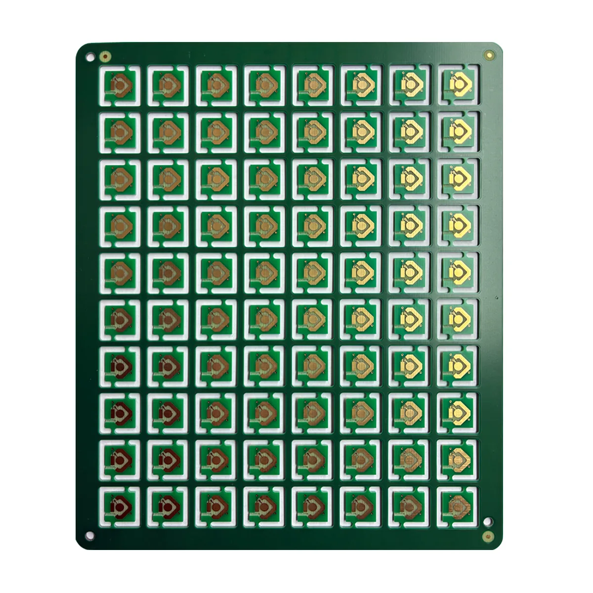
| Finitura superficiale | QUALSIASI 2h” + Oro duro 30u” (Doppia protezione: Oro per immersione chimica + Oro elettrolitico per resistenza all'usura) |
| Peso del rame | 1oz (35μm) (Spessore standard, sufficiente per la maggior parte dei requisiti di trasporto di corrente) |
| Maschera di saldatura | Verde (Predefinito; Nero, Blu, Rosso, Bianco disponibile su richiesta) |
| Silkscreen | Inchiostro epossidico bianco (Identificatori dei componenti, Logo) |
| Min. Foro | 0.3mm (12mil) |
| Min. Larghezza/Spazio della linea | 3mil / 3mil |
Iii. Definizione del prodotto: Cos'è un PCB rigido a 2 strati?
1. Definizione
UN PCB rigido è un circuito stampato non flessibile composto da un substrato, tracce di lamina di rame, maschera di saldatura, e serigrafia. Stabilisce collegamenti elettrici fissi attraverso processi di foratura e incisione.
UN 2-PCB rigido a strati (Tavola bifacciale) è il tipo fondamentale di PCB rigido, presenta tracce di rame su entrambi i lati superiore e inferiore del substrato. I collegamenti elettrici tra gli strati vengono ottenuti tramite Fori passanti placcati (Via).
2. Classificazione per numero di strati
- 1-Strato (Monofacciale): Circuiti su un solo lato. Costo più basso ma gravi limitazioni di routing.
- 2-Strati (Doppia faccia): Circuiti su entrambi i lati. Maggiore flessibilità di routing rispetto a un solo lato; costo moderato. (La specialità dell'UGPCB)
- Multistrato (4+ Strati): Tre o più strati di rame. Adatto a circuiti complessi ma dal costo notevolmente più elevato.
L’offerta a 2 livelli di UGPCB rappresenta il il più alto rapporto costo-prestazioni nella categoria PCB rigidi.
IV. Linee guida di progettazione per l'alta affidabilità
Con spazio di routing limitato su schede a 2 strati, aderendo a IPC-2221 Gli standard di progettazione sono cruciali per l'integrità del segnale e la gestione termica.
1. Alimentazione e layout di terra
- Piani terrestri: Utilizzare grandi colate di rame per il terreno (GND) per ridurre al minimo le interferenze del segnale e le EMI.
- Tracce di potere: Ampliare le tracce VCC a >20mil per ridurre la resistenza e la caduta di tensione.
- Spaziatura: Mantenere un minimo 10autorizzazione mil tra alimentazione e terra per migliorare il filtraggio.
2. Instradamento del segnale
- Coppie differenziali: Per segnali ad alta frequenza (USB, HDMI), utilizzare un percorso differenziale per ridurre la radiazione elettromagnetica.
- 3Regola W: Mantenere una spaziatura di ≥3 volte la larghezza della traccia tra le linee del segnale per evitare diafonia.
- Percorsi di ritorno: Evitare che le tracce del segnale attraversino le fessure del piano di terra per evitare la riflessione del segnale.
3. Tramite Design
- Dimensione del foro: Ridurre al minimo il diametro (per esempio., 0.3mm) per risparmiare spazio di routing.
- Tramite tenda: Utilizzare la maschera di saldatura per coprire le vie per impedire l'assorbimento della pasta saldante durante la saldatura.
- Alta frequenza: Utilizzare via a foro passante (standard per 2 strati) per ridurre al minimo la capacità parassita rispetto ai via ciechi/sepolti.
V. Principio di funzionamento: Come funzionano i PCB
La funzione principale di un PCB è collegare componenti elettronici (patatine, resistori, condensatori) tramite tracce di rame per ottenere funzioni elettriche predeterminate.
- Esempio: In una scheda di ricarica per smartphone, il PCB instrada l'alimentazione dall'interfaccia USB al chip di gestione della ricarica, lo distribuisce alla batteria, e restituisce i dati sul livello della batteria al sistema tramite linee di segnale.
- Mentre il principio è identico a pannelli multistrato, 2-le tavole a strati richiedono una meticolosa pianificazione del layout per garantire Integrità del segnale (E) all'interno di uno spazio limitato.
VI. Materiale & Prestazione: Perché FR-4 TG150?
1. Materiale di base: FR-4TG150
FR-4 (Ritardante di fiamma 4) è lo standard industriale per i substrati in tessuto di vetro in resina epossidica.
- Elevata resistenza meccanica: Rinforzato con tessuto di vetro, resistere alla flessione e alla rottura.
- Stabilità termica: TG150 (Temperatura di transizione vetrosa 150°C) garantisce stabilità in ambienti ad alta temperatura (officine industriali, vani motore automobilistici).
- Proprietà elettriche: Costante dielettrica (Non so) 4.2-4.5, Fattore di dissipazione (Df) 0.02, rendendolo adatto alla trasmissione di segnali ad alta frequenza.
- Resistenza chimica: Resiste alla corrosione da saldatura e flusso, prolungare la vita utile.
2. Finitura superficiale: QUALSIASI 2h” + Oro duro 30u”
La finitura superficiale funge da PCB “scudo protettivo.” UGPCB combina due finiture per il massimo beneficio:
- Essere d'accordo (Oro per immersione in nichel chimico): UN 2tu” (0.05μm) strato d'oro depositato chimicamente. Offre eccellente planarità e saldabilità, ideale per componenti a passo fine (per esempio., 0.5trucioli con passo mm).
- Oro duro (Oro elettrolitico): Uno spesso 30tu” (0.76μm) strato d'oro placcato elettricamente. Fornisce resistenza all'usura e conduttività superiori, perfetto per frequenti cicli di collegamento/scollegamento (Porte USB, Slot per schede SD).
Confronto: Questa combinazione supera HASL (Livellamento della saldatura ad aria calda) e OSP standard (Conservante organico di saldabilità) in applicazioni ad alta affidabilità come controllo industriale E elettronica automobilistica.
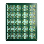
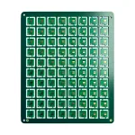
VII. Struttura & Caratteristiche: Vantaggi della pannellatura
Questo PCB utilizza Pannellizzazione della matrice, dove più singoli PCB (per esempio., 10×10 vettore) sono disposti su un pannello di produzione più grande collegato da Reti (Schede).
Vantaggi della pannellatura:
- Efficienza produttiva: Più PCB prodotti simultaneamente, riducendo i tempi di setup della macchina.
- Riduzione dei costi: Riduce al minimo il materiale di scarto e massimizza l'utilizzo del materiale.
- Facilità di montaggio: I nastri possono essere separati tramite instradamento o Taglio a V (Punteggio V) senza danneggiare le singole tavole.
Ulteriori caratteristiche del prodotto:
- Alta affidabilità: FR-4TG150 + ENIG/Hard Gold resiste ad ambienti difficili (alta temperatura, umidità, vibrazione).
- Basso costo: Il processo maturo a 2 strati è 30%-50% più economico rispetto ai pannelli multistrato.
- Personalizzazione: Supporta min. 0.1dimensione del foro mm, min. 3mil traccia/spazio, e varie finiture (Argento immersione, OSP, ecc.).
- Ecologico: Conforme a RoHS E PORTATA standard; saldatura senza piombo pronta per l'esportazione globale.
VIII. Processo di produzione: Rigoroso IPC-A-600 & Controllo IPC-6012
Il flusso di lavoro di UGPCB aderisce rigorosamente a IPC-A-600 (Norma di qualità) E IPC-6012 (Specifiche prestazionali per PCB rigidi).
- Taglio: Taglio del laminato FR-4 alle dimensioni richieste (per esempio., 18″x24″).
- Perforazione: Foratura CNC per fori componenti (0.3mm) e via (0.2mm).
- Rame chimico: Deposizione chimica di rame da 1-2μm per la connettività tra strati.
- Trasferimento di immagini: Applicazione del fotoresist, esponendo, e lo sviluppo per trasferire modelli di circuito.
- Incisione: Rimozione del rame in eccesso per formare tracce finali.
- Maschera di saldatura: Rivestimento con inchiostro verde per maschera di saldatura, esponendo, e polimerizzazione per proteggere i circuiti.
- Finitura superficiale: Essere d'accordo (2tu”) + Oro duro (30tu”) placcatura per saldabilità.
- Silkscreen: Designatori dei componenti di stampa (R1, C2) e loghi.
- Prova elettrica: Test della sonda volante per verificare la continuità e l'isolamento (niente pantaloncini/aperture).
- Instradamento/Taglio a V: Separazione dei singoli PCB dal pannello e smussatura dei bordi.
- Ispezione finale: AOI (Ispezione ottica automatizzata) per graffi, ossidazione, precisione dimensionale, e test di affidabilità (Shock termico, Vibrazione).
IX. Scenari di applicazione
Grazie alla sua elevata affidabilità e convenienza, questo PCB è ampiamente utilizzato in:
- Elettronica di consumo
- Cellulari/Tablet: Schede di ricarica, moduli di potenza, tastiere.
- Indossabili: Schede madri per smartwatch, sensori del fitness tracker.
- Elettrodomestici: Schede di controllo AC, display della lavatrice.
- Controllo industriale
- Moduli PLC: Schede I/O, moduli di comunicazione.
- Sensori: Elaborazione del segnale per sensori di temperatura/pressione.
- Robotica: Controllo del servomotore, interfacce dell'encoder.
- Elettronica automobilistica
- Infotainment: Schede madri di navigazione, controlli audio.
- Sistemi di sicurezza: Controllo radar inverso, TPMS (Monitoraggio della pressione dei pneumatici).
- Veicoli elettrici: Controllo della pila di ricarica, BMS (Sistema di gestione della batteria) tavole ausiliarie.
- Dispositivi medici
- Diagnostica portatile: Misuratori di glucosio, sfigmomanometri.
- Monitoraggio: ECG, schede di segnalazione del pulsossimetro.
- Chirurgico: Schede di controllo per strumenti mininvasivi.
- Altri campi
- Telecom: Schede di interfaccia router/switch.
- Aerospaziale: Controllori di volo dei droni, comunicazioni satellitari.
- Casa intelligente: Serrature intelligenti, controlli di illuminazione intelligenti.
X. Perché scegliere UGPCB?
Come produttore professionale di PCB con oltre 10 anni di esperienza, UGPCB serve 1000+ clienti a livello globale.
- Attrezzature avanzate: Trivelle giapponesi Mitsubishi, Macchine per esposizione LPKF tedesche, Ricerca sui test statunitensi tester a sonde volanti.
- Qualità rigorosa: Certificato con ISO9001, ISO14001, e IATF16949 (Industria automobilistica).
- Tempi di consegna rapidi: 24-tempo di consegna di un'ora per prototipi; 3-5 giorni per la produzione in serie.
- Servizi gratuiti: DFM (Progettazione per la produzione) Controllo, preventivi gratuiti, e test campione gratuiti (per i primi ordini).
XI. Richiedi un preventivo: Accelera il tuo time-to-market
Se hai bisogno 2-PCB FR-4 rigidi a strati o hai domande su ENIG+Oro duro O pannellatura, contatta UGPCB oggi stesso!
- ✅ Recensione DFM gratuita: Ottimizza il tuo progetto per prevenire difetti di produzione.
- ✅ Test campione gratuito: Verificare le prestazioni prima della produzione di massa.
- ✅ Prezzi competitivi: Soluzioni economicamente vantaggiose basate su quantità e specifiche.
- ✅ Consegna rapida: Prototipi in 24h, Produzione di massa nel 3-5 giorni.
Riepilogo
UGPCB 2-PCB FR-4 rigido a strati, caratterizzato Materiale base FR-4 TG150 E Essere d'accordo + Finitura superficiale in oro duro, è la scelta migliore per le applicazioni più impegnative alta affidabilità E basso costo. Che tu sia un produttore di elettronica di consumo o un ingegnere automobilistico, forniamo soluzioni personalizzate che soddisfano Norme IPC-A-600.
Contattaci subito per avviare il tuo progetto e cogliere le opportunità di mercato!


