
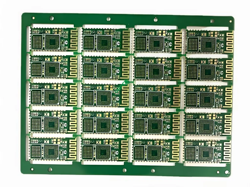
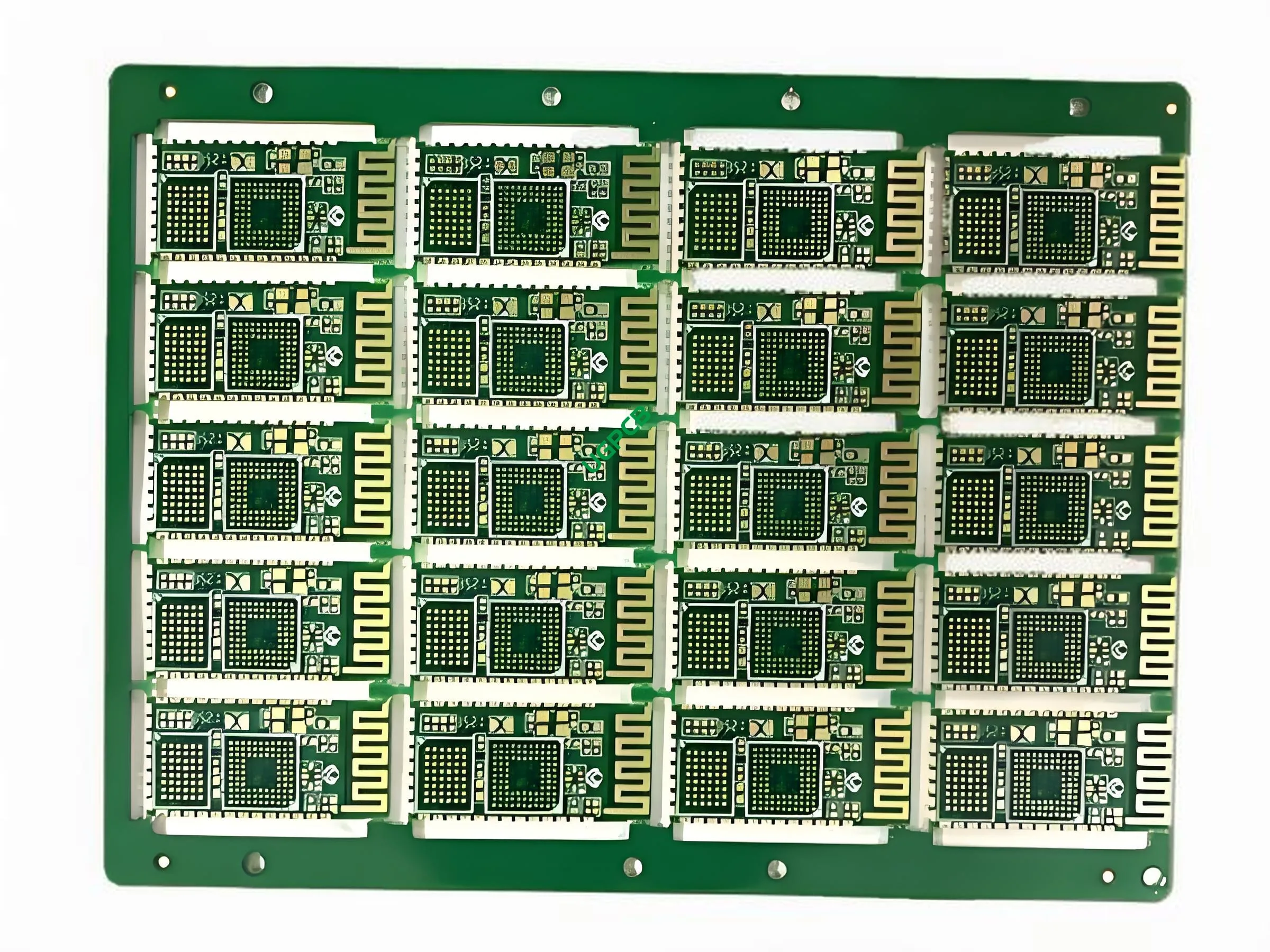
Half Hole WiFi Module PCB: A Comprehensive Overview
The Half Hole WiFi Module PCB is a sophisticated electronic component designed to facilitate seamless Wi-Fi connectivity in various devices. This module combines the advantages of both surface mount and through-hole technology, making it highly versatile for diverse applications.
Definizione
A Half Hole WiFi Module PCB refers to a circuito stampato (PCB) that incorporates components with both surface mount (SMD) and through-hole (THD) technologies. It is specifically engineered to support Wi-Fi modules, enabling efficient wireless communication.
Requisiti di progettazione
The design of this PCB adheres to stringent requirements to ensure optimal performance:
- Materiale: High-quality FR4, noto per le sue eccellenti proprietà elettriche e durata.
- Strati: Four layers to accommodate complex circuitry while maintaining compactness.
- Colore: Available in Black and White, providing aesthetic flexibility.
- Spessore finito: 1.0mm to strike a balance between robustness and space efficiency.
- Spessore del rame: 1OZ, ensuring reliable conductivity.
- Trattamento superficiale: Immersione oro per migliorare la saldabilità e la resistenza alla corrosione.
- Min Trace/Space: 4mil(0.1mm), allowing for fine detailing and high-density layouts.
Principio di lavoro
The Half Hole WiFi Module PCB operates by integrating with Wi-Fi modules to provide wireless communication capabilities. It uses embedded antennas and radio-frequency (Rf) components to transmit and receive data over Wi-Fi networks. The surface mount components offer high-speed signal processing, while the through-hole components ensure stable mechanical connections.
Applicazioni
This PCB is widely used in:
- Dispositivi IoT: Enabling smart home appliances and industrial equipment to connect wirelessly.
- Elettronica di consumo: Integrating Wi-Fi functionality into gadgets like smart TVs and gaming consoles.
- Sistemi automobilistici: Supporting infotainment systems and advanced driver assistance features.
- Attrezzatura medica: Facilitating remote monitoring and diagnostic tools.

Types and Classification
The Half Hole WiFi Module PCB can be classified based on several criteria:
- Per tecnologia: Combination of SMD and THD.
- Per applicazione: General purpose or specific use cases like automotive or medical.
- By Frequency Band: Supporting 2.4GHz, 5GHz, or dual-band operations.
Composizione materiale
Constructed primarily from FR4, Questo Materiale PCB offers:
- Superior thermal stability
- High mechanical strength
- Excellent electrical insulation properties
Performance Metrics
Key performance indicators include:
- Integrità del segnale: Maintained through careful layout design and impedance matching.
- Affidabilità: Ensured by rigorous testing protocols and quality control measures.
- Compatibilità: With a wide range of Wi-Fi standards including 802.11 b/g/n/ac.
Caratteristiche strutturali
The PCB’s structure comprises:
- Multilayer stackup for enhanced signal integrity
- Precision-etched traces and spaces for fine circuitry
- Robust through-hole plating for durable mechanical connections
Distinctive Traits
Notable characteristics include:
- Versatility in mounting options (SMD and THD)
- High signal-to-noise ratio due to optimized layout
- Resistenza a fattori ambientali come l'umidità e le variazioni di temperatura
Flusso di lavoro di produzione
Il processo di produzione prevede diverse fasi:
- Progettazione e impaginazione: Using advanced CAD software to create precise schematics.
- Preparazione del materiale: Cutting FR4 sheets to size and cleaning them thoroughly.
- Incisione: Applying etchant to remove unwanted copper from the board.
- Placcatura: Immersing the board in a gold bath for surface finishing.
- Assemblaggio: Soldering surface mount and through-hole components accurately.
- Test: Conducting functional tests to ensure compliance with specifications.
- Controllo di qualità: Final inspection for defects and performance validation.
Casi d'uso
Typical scenarios where this PCB finds application include:
- Smart Home Automation Systems
- Portable Medical Diagnostic Tools
- In-vehicle Communication Networks
- Industrial Machinery with Wireless Connectivity Needs
In sintesi, the Half Hole WiFi Module PCB stands out as an innovative solution catering to the growing demand for reliable wireless communication in various sectors. Its unique blend of SMD and THD technologies, along with rigorous design and manufacturing standards, ensures top-notch performance and broad applicability.


