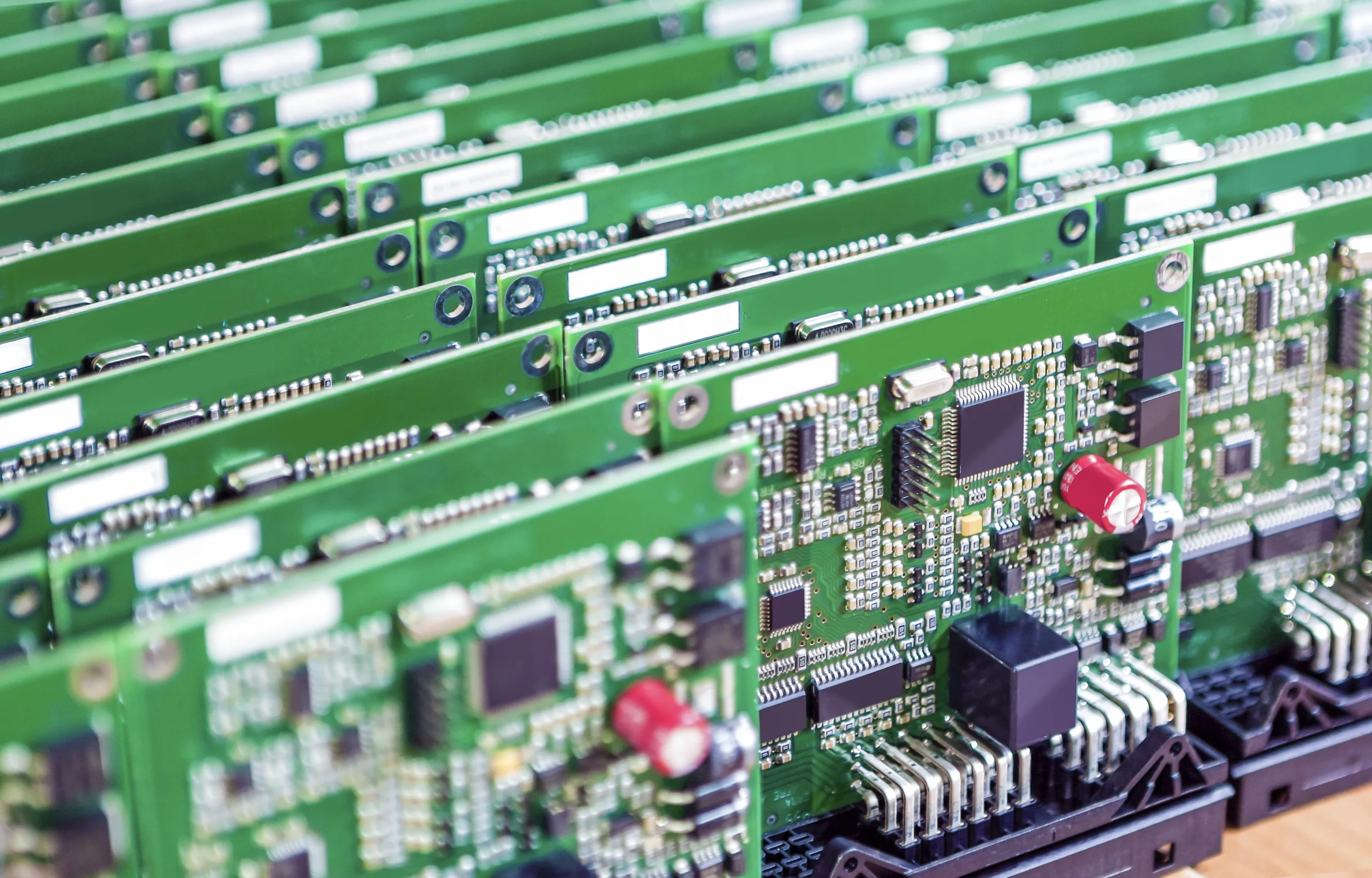
Definizione di PCB multistrato
Un PCB multistrato è un circuito con più di due strati. A differenza dei PCB a doppia faccia, che hanno solo due strati di materiale conduttivo, tutti i PCB multistrato devono avere almeno tre strati di materiale conduttivo sepolto al centro del materiale.
Struttura del PCB multistrato
Combinazione di diversi strati
Come suggerisce il nome, un PCB multistrato è una combinazione di diversi strati. Un PCB a singola faccia e un PCB a doppia faccia si combinano per formare un PCB dal design complesso. I PCB multistrato aumentano il numero di strati e quindi aumentano l'area disponibile per il routing. Queste schede sono realizzate combinando PCB a due strati e separandoli con materiali isolanti come i dielettrici.
Numero di strati conduttivi
Gli strati conduttivi tra i materiali isolanti sono almeno tre, e possiamo incorporare fino a cento strati secondo necessità. Trattiamo i PCB multistrato come PCB rigidi perché è difficile produrre PCB multistrato flessibili. La maggior parte dei nostri comuni PCB multistrato sono costituiti da 4 A 8 strati. Gli smartphone possono contenere fino a 12 livelli in base alla complessità dell'applicazione. I produttori preferiscono gli strati con numeri pari a quelli con numeri dispari, perché la laminazione di strati dispari può rendere il circuito eccessivamente complesso e problematico, e anche il costo elevato è un fattore da considerare.
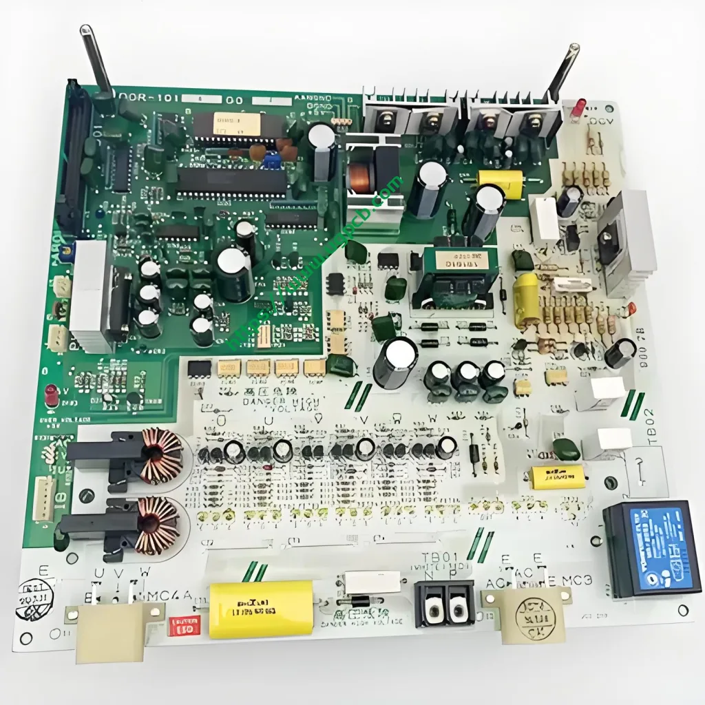
Vantaggi del PCB multistrato
I PCB multistrato presentano alcuni vantaggi rispetto ai PCB a strato singolo o doppio. Hanno densità più elevate, consentendo una maggiore funzionalità, capacità e velocità. La schermatura elettromagnetica è più semplice se i piani di alimentazione e di terra sono posizionati correttamente. Non è richiesto alcun cablaggio esteso, quindi è leggero. Riducono le dimensioni e aiutano a risparmiare spazio. Sono più flessibili rispetto ad altri tipi di PCB.
Applicazioni del PCB multistrato
I PCB multistrato hanno molte applicazioni. Questi includono:
-
Computer
-
Ricevitori in fibra ottica
-
Archiviazione dei dati
-
Trasmissione del segnale
-
Trasmissione da telefono cellulare
-
Ripetitori di telefoni cellulari
-
Tecnologia GPS
-
Controllo industriale
-
Sistemi satellitari
-
Dispositivi portatili
-
Attrezzatura di prova
-
Apparecchiature a raggi X
-
Monitor cardiaci
-
Tecnologia di scansione CAT
-
Acceleratori atomici
-
Sistemi centrali di allarme antincendio
-
Sistemi di rilevamento nucleare
-
Apparecchiature per il rilevamento spaziale
-
Attrezzatura per l'analisi meteorologica


