

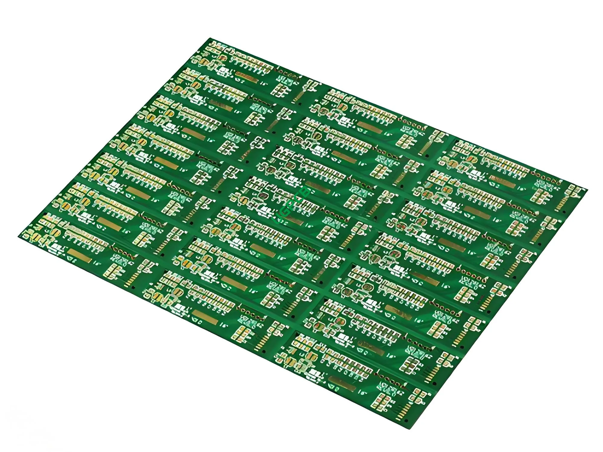
Panoramica del circuito stampato LED P2.9
Il circuito stampato P2.9 LED (PCB) è specializzato PCB Progettato per l'uso con moduli LED P2.9, che sono comunemente usati nelle applicazioni di visualizzazione ad alta risoluzione. Questo PCB è ideale per creare grandi, display a LED senza soluzione di continuità.
Cos'è un circuito stampato a LED P2.9?
Un circuito stampato a LED P2.9 è un circuito stampato (PCB) Progettato specificamente per ospitare e collegare i moduli LED P2.9. Il termine “P2.9” si riferisce al pixel pitch del modulo LED, che misura 2.9 millimetri tra ogni pixel. Questo PCB garantisce che i moduli a LED possano essere interconnessi in modo efficiente, Fornire una piattaforma stabile per i componenti elettronici.
Requisiti di progettazione
I requisiti di progettazione per un circuito stampato a LED P2.9 sono rigorosi per garantire le prestazioni e l'affidabilità:
- Materiale: SY1000-2 TG170 FR4, scelto per le sue eccellenti proprietà elettriche e termiche.
- Conta dei strati: 6 strati per adattarsi ai circuiti necessari e all'integrità del segnale.
- Colore: Nero/nero per facile identificazione e fascino estetico.
- Spessore finito: 1.0mm per fornire integrità strutturale e durata.
- Spessore del rame: 1Oz per garantire una conducibilità adeguata e dissipazione del calore.
- Trattamento superficiale: Immersione oro per migliorare la saldabilità e la resistenza alla corrosione.
- Traccia e spazio minimi: 4mil(0.1mm) Per supportare i modelli di circuito fine.
- Caratteristica: Altri cuscinetti con piccola spaziatura per adattarsi al layout denso dei moduli LED P2.9.
Come funziona?
Il circuito stampato a LED P2.9 funziona fornendo una piattaforma per vari componenti elettronici da interconnettere attraverso percorsi conduttivi. Questi percorsi, o tracce, sono realizzati in rame e sono incisi sul tabellone. Il materiale SY1000-2 TG170 FR4 garantisce che il PCB possa resistere alle esigenze delle applicazioni di visualizzazione a LED, Mentre il trattamento della superficie dell'oro immersione garantisce che queste tracce rimangano conduttive e resistenti alla corrosione.
Applicazioni
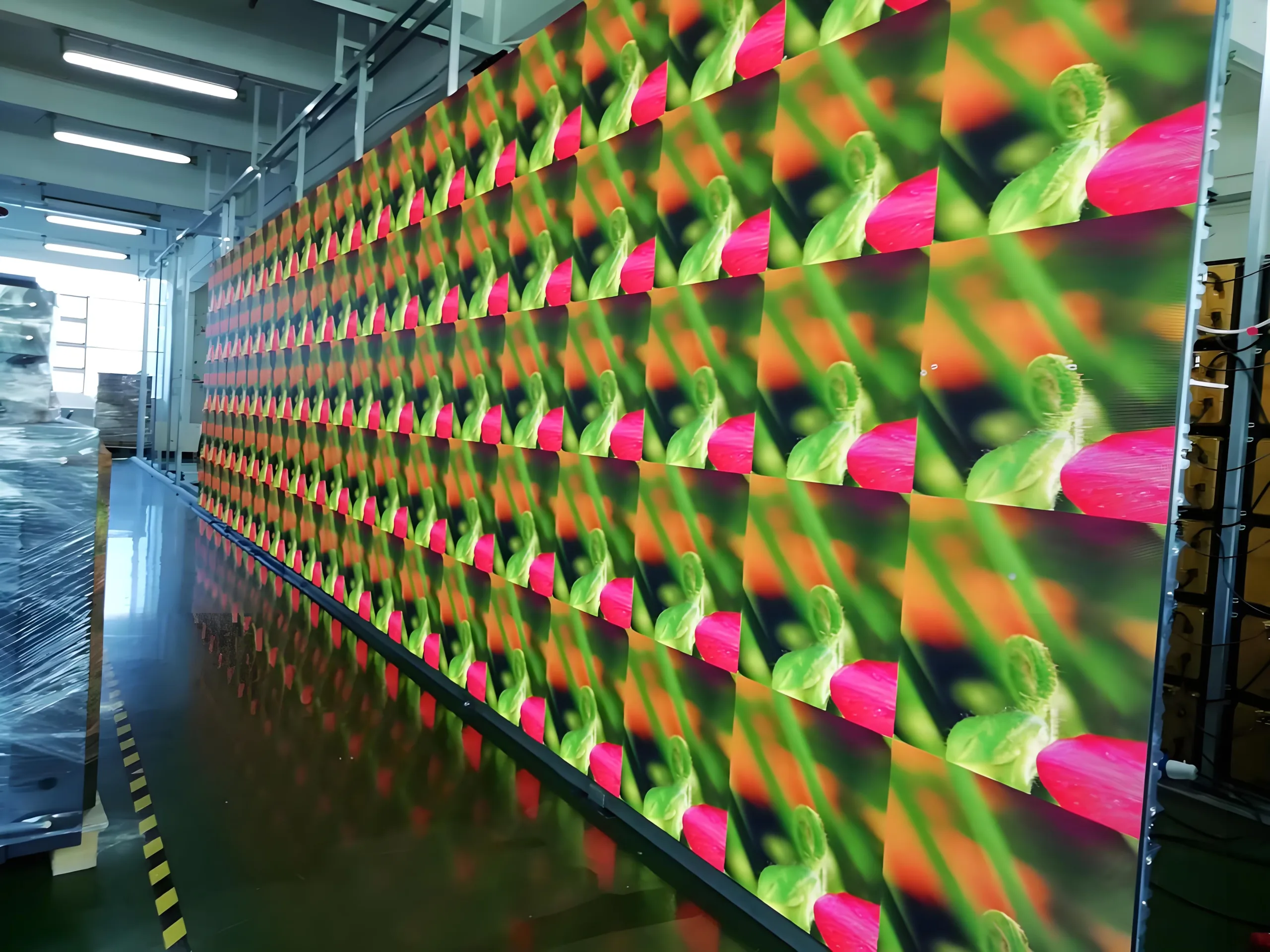
L'applicazione primaria del circuito stampato a LED P2.9 è in sistemi di visualizzazione a LED ad alta risoluzione in cui gestisce e regola il flusso di segnali elettrici. Questo include:
- Display a LED interni ed esterni
- Segnaletica digitale
- Pareti video di grande formato
- Fase di eventi e schermate di concerti
Classificazione
Basato sulle sue caratteristiche e applicazioni, Il circuito stampato a LED P2.9 può essere classificato come ad alta densità, PCB digitale ad alta velocità Progettato per applicazioni di visualizzazione a LED. Questa classificazione evidenzia la sua capacità di gestire segnali ad alta frequenza e fornire connessioni elettriche stabili.
Composizione materiale
Il nucleo materiale Utilizzato nel circuito stampato P2.9 LED è SY1000-2 TG170 FR4, Un materiale composito ad alte prestazioni noto per il suo eccellente meccanico, termico, e proprietà elettriche. Questo materiale garantisce che il PCB possa resistere alle esigenze delle applicazioni di visualizzazione a LED.
Caratteristiche delle prestazioni
Le caratteristiche delle prestazioni del circuito stampato a LED P2.9 includono:
- Alta integrità del segnale
- Bassa perdita di segnale
- Gestione termica superiore
- Solida resistenza meccanica
- Stabilità a lungo termine
Dettagli strutturali
I dettagli strutturali del circuito stampato a LED P2.9 sono i seguenti:
- Conta dei strati: 6 strati
- Spessore finito: 1.0mm
- Spessore del rame: 1OZ
- Trattamento superficiale: Oro ad immersione
- Traccia e spazio minimi: 4mil(0.1mm)
- Caratteristica: Altri cuscinetti con piccola spaziatura per adattarsi al layout denso dei moduli LED P2.9.
Caratteristiche e vantaggi
Le caratteristiche chiave e i vantaggi del circuito stampato a LED P2.9 includono:
- Interconnettività ad alta densità
- Ottima integrità del segnale
- Solida costruzione meccanica
- Prestazioni affidabili a lungo termine
- Opzioni di colore estetico (Bianco/nero)
Processo di produzione
Il processo di produzione del circuito stampato a LED P2.9 prevede diversi passaggi tra cui:
- Selezione del materiale: Scegliere materiale SY1000-2 TG170 FR4 di alta qualità.
- Stacking strato: Organizzare il 6 strati con precisione.
- Incisione: Rimozione del rame in eccesso per formare i modelli di traccia desiderati.
- Applicazione della maschera di saldatura: Applicazione di uno strato di maschera di saldatura per proteggere le tracce di rame.
- Placcatura: Applicazione del trattamento della superficie dell'oro immersione.
- Assemblaggio: Incorporare PTH e VIA per interconnessioni di livello.
- Test: Garantire che il PCB soddisfi tutte le specifiche delle prestazioni.
Casi d'uso
Il circuito stampato a LED P2.9 viene utilizzato in vari scenari come:
- Display a LED interni ed esterni ad alta risoluzione
- Installazioni di segnaletica digitale
- Fase di concerti ed eventi con grandi pareti video
- Ambienti di vendita al dettaglio con schermi pubblicitari dinamici


