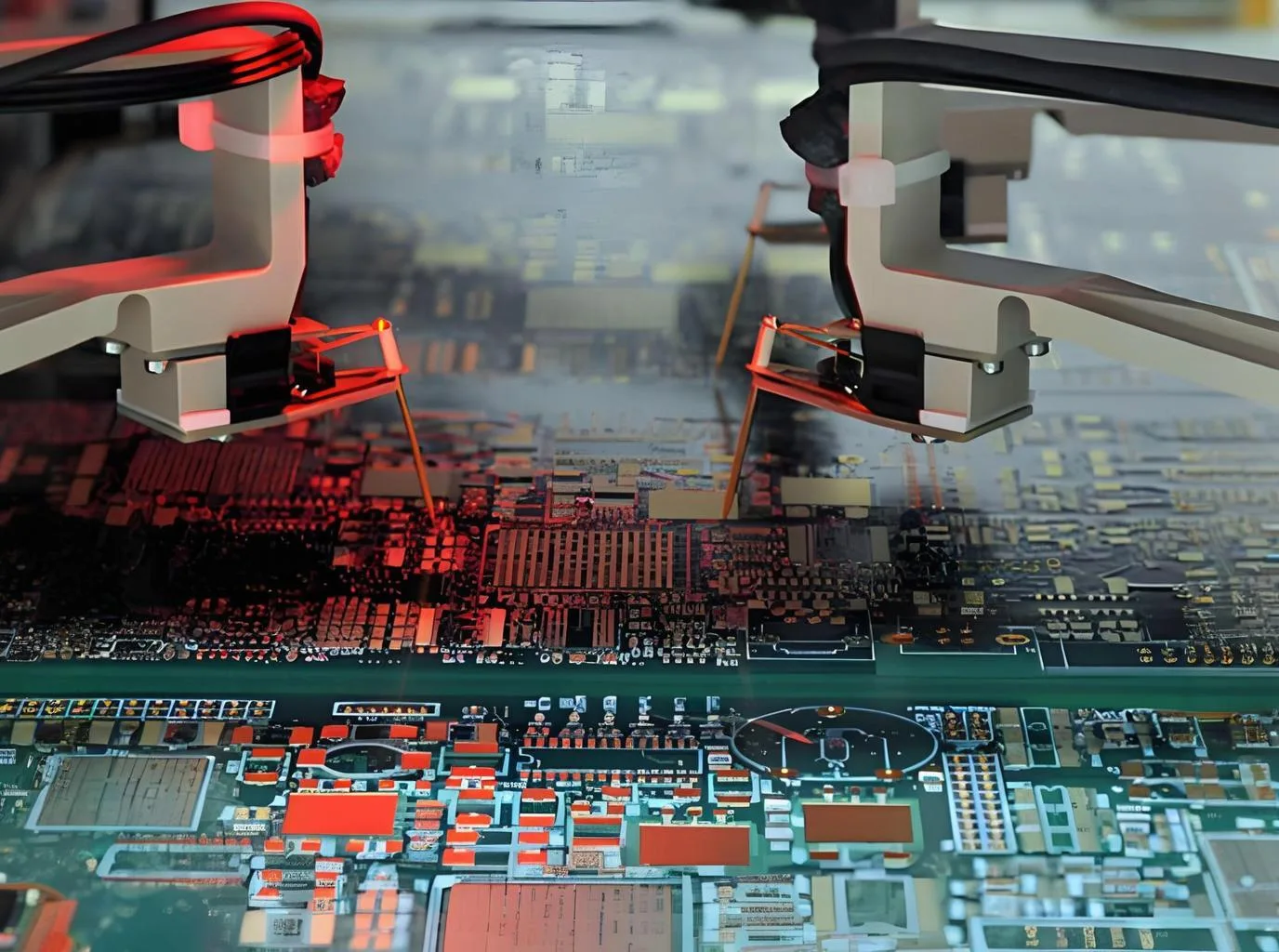
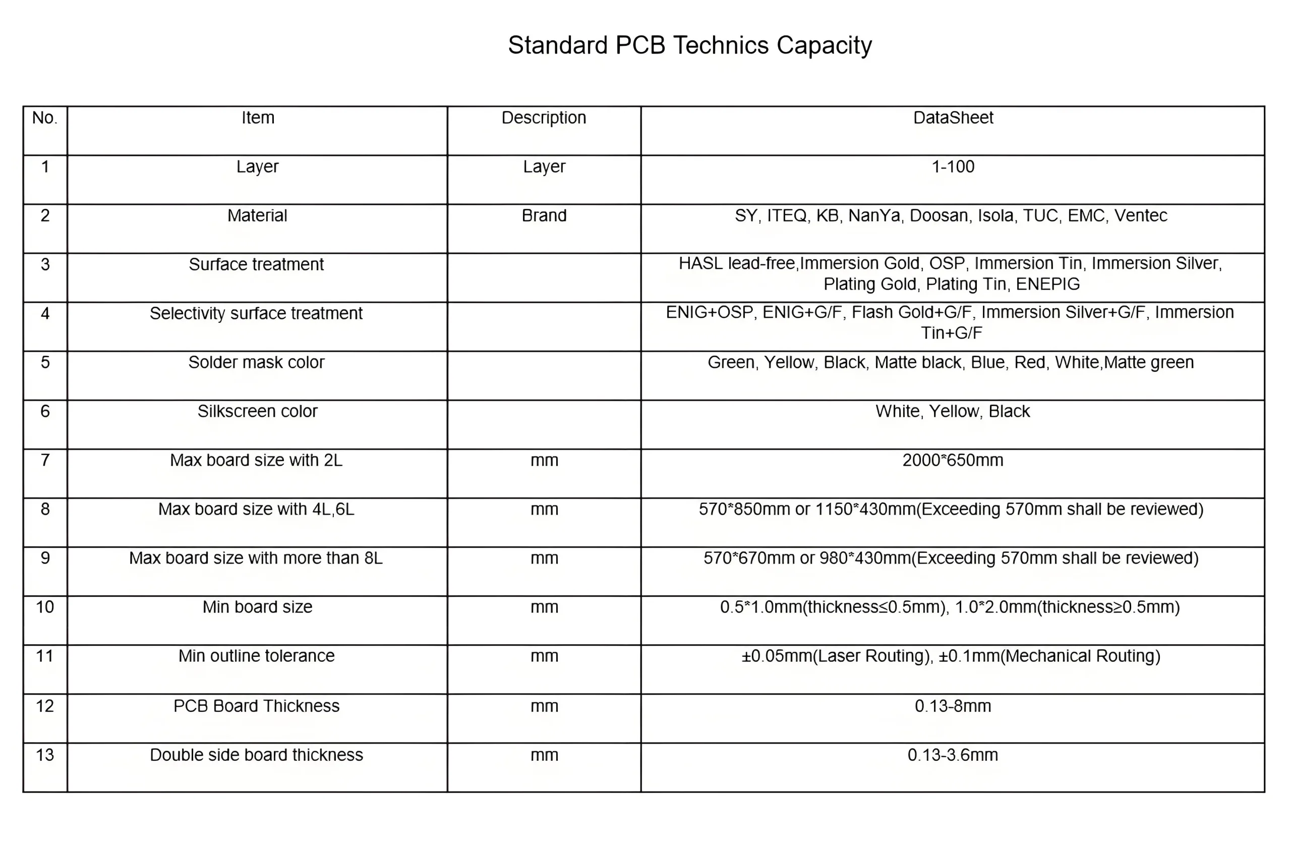
高精度回路イメージング & エッチング技術
UGPCB Factory は、回路パターニングとエッチングにおける優れたプロセス制御を実証します. 標準的な PCB 製造用, 私たちは一貫して達成します:
- レーザー直接イメージング (LDI) 従来のフォトリソグラフィマスクを置き換える, ±5μmのアライメント精度でデジタルファイルベースの露光を可能にします
- アルカリエッチング処理 ±15%の線幅制御によりきれいなラインエッジを確保 (業界をリードする耐性)
- さまざまな厚さの銅を扱う専門知識 (1oz-6oz) サイドエッチングを最小限に抑えた
高精度穴あけ加工 & ホールメタライゼーション
当社の掘削能力は以下をカバーします:
- 機械掘削 穴サイズ公差±0.025mmの0.4mm~3.0mm基板用
- レーザー掘削 最小0.1mmのマイクロビア
- ホールメタライゼーション 達成 >20高度な化学蒸着と電気めっきによるμmの均一な銅めっき
- 特別なプロセス 8:1 に 10:1 アスペクト比の要件
多層ラミネート & 層間配向
- FR-4 グレード A 材料を使用した最大 100 層の PCB 製造
- ±15umの層間アライメントによる高精度ラミネート
- 温度/圧力/時間制御されたプロセスにより層間剥離を防止
- 高Tg材料のオプション, 高速ラミネート, 1000μmまでの重銅
はんだマスク & 表面仕上げオプション
- はんだマスクの色: 緑/青/赤/黒、最小0.08mmのはんだブリッジ付き
- 表面仕上げ:
- 出血 (熱気はんだレベリング)
- 同意する (エレクトロレスニッケルイマージョンゴールド)
- 浸漬錫/銀
- OSP (有機はんだ付け性防腐剤)
総合的なQC & 試験システム
- AOI検査: ライン/スペースの高解像度欠陥検出, パッド, ショートパンツ/オープンパンツ
- インピーダンス制御: 高速/RF アプリケーション向けの許容誤差は ±10%
- 電気テスト: 飛行プローブ & フィクスチャベースの導通検証
- 信頼性試験: サーマルショック, 耐湿性, 曲げ試験
プロセス能力 & 安定性
- CPK >1.33 (4a) 重要なプロセス全体にわたって, 到達 1.67 (5a) 主要な分野で
- 線幅制御±15%以内 (対業界 20% 標準)
- 統計的プロセス管理 (SPC) 一貫した生産品質の確保
PCBAワンストップサービス
- SMTアセンブリ: 01005 ±0.03mmの配置精度でのコンポーネント処理
- 高度なパッケージ: X線検査によるBGA/Micro BGA/PoPのサポート
- DFM サポート: インピーダンスの計算, スタックアップデザイン, 製造可能性分析
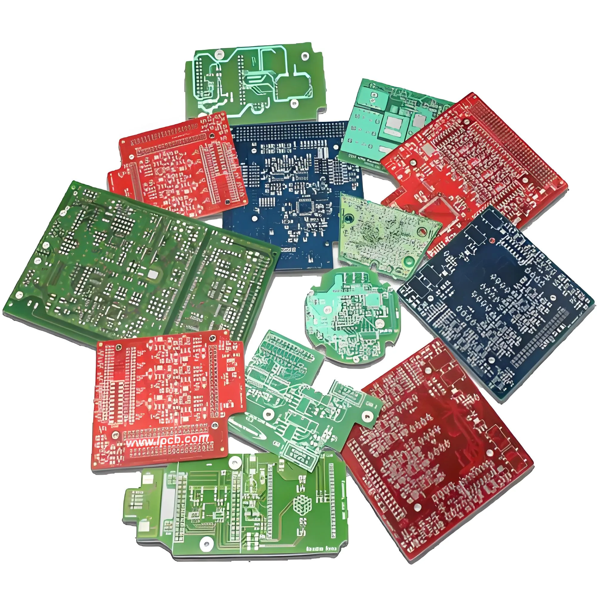
業界アプリケーション & 接触
家庭用電化製品の提供, 産業用制御, 通信, 医療機器, カスタマイズされた PCB ソリューションを備えた自動車分野. 工程能力レポートと無料の DFM コンサルティングについては、当社の Web サイトにアクセスしてください。.
微信
WeChat で QR コードをスキャンします