
電子機器を再構築する静かな物質革命
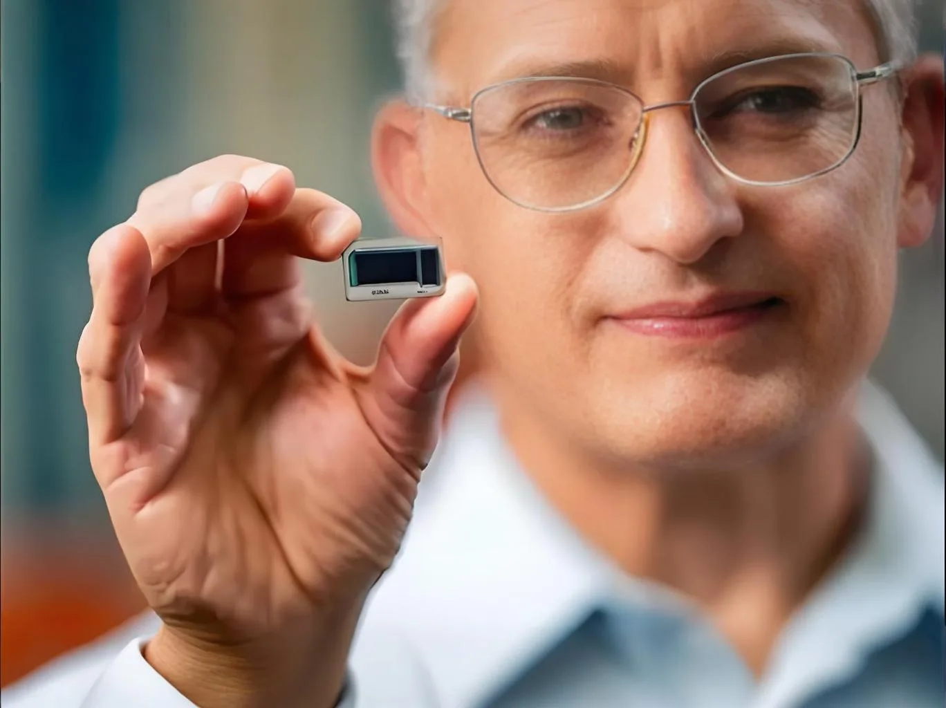
インテル 2024 グラスのグローバルデビュー 基板パッケージ テクノロジーは、半導体製造の地震シフトを爆発させました. で 2025 蘇州TGV Industry Summit, Intelの技術リーダー, TSMC, そしてサムスンは同意した: “ガラス基板は半導体パッケージングを「透明な時代」に駆り立てます,’ 市場の浸透を超えています 50% 5年以内。” この分析では、技術的根拠を探ります, 産業チェーン変換, とへの影響 プリント基板 産業.
1. 技術的な優位性: ガラス基板がパッケージを再定義する理由
1.1 物理的な財産の支配
比較分析により、ガラス基質が明らかになります’ 圧倒的な利点 :
| パラメーター | 有機基板 | シリコンインターポーザー | ガラス基板 |
|---|---|---|---|
| 誘電率 | 4.2-4.8 | 11.9 | 3.9 |
| 損失の接線 | 0.02-0.04 | 0.001-0.01 | 0.0001-0.001 |
| CTE (ppm/°C) | 16-18 | 2.6 | 3.2-7.5 (調整可能) |
| 熱伝導率 | 0.2-0.3 | 150 | 1.1 |
| 表面の粗さ | 0.5-1.0 μm | 0.05 μm | <0.01 μm |
(ソース: Intel技術ホワイトペーパー, コーニングマテリアルラボ)
信号損失方程式分析
減衰 (a) として定義されています:

ε'≈3.9およびεで”ガラス基板の場合≈0.001, 高周波 (100GHz) 損失は減少します 67% 対有機基質 (E'4.5, e”≈0.03).
1.2 指数密度の向上
NvidiaのGB200 GPUが実証しています 50%+ ガラス基板を使用してダイカウント増加, 5μm/5μm配線密度を達成します:
-
原子レベルの平坦性 (<0.01μm粗さ)
-
調整可能なCTEマッチング (3ppm/°C)
-
機械的安定性 (700×700mmパネルの反り <50μm)
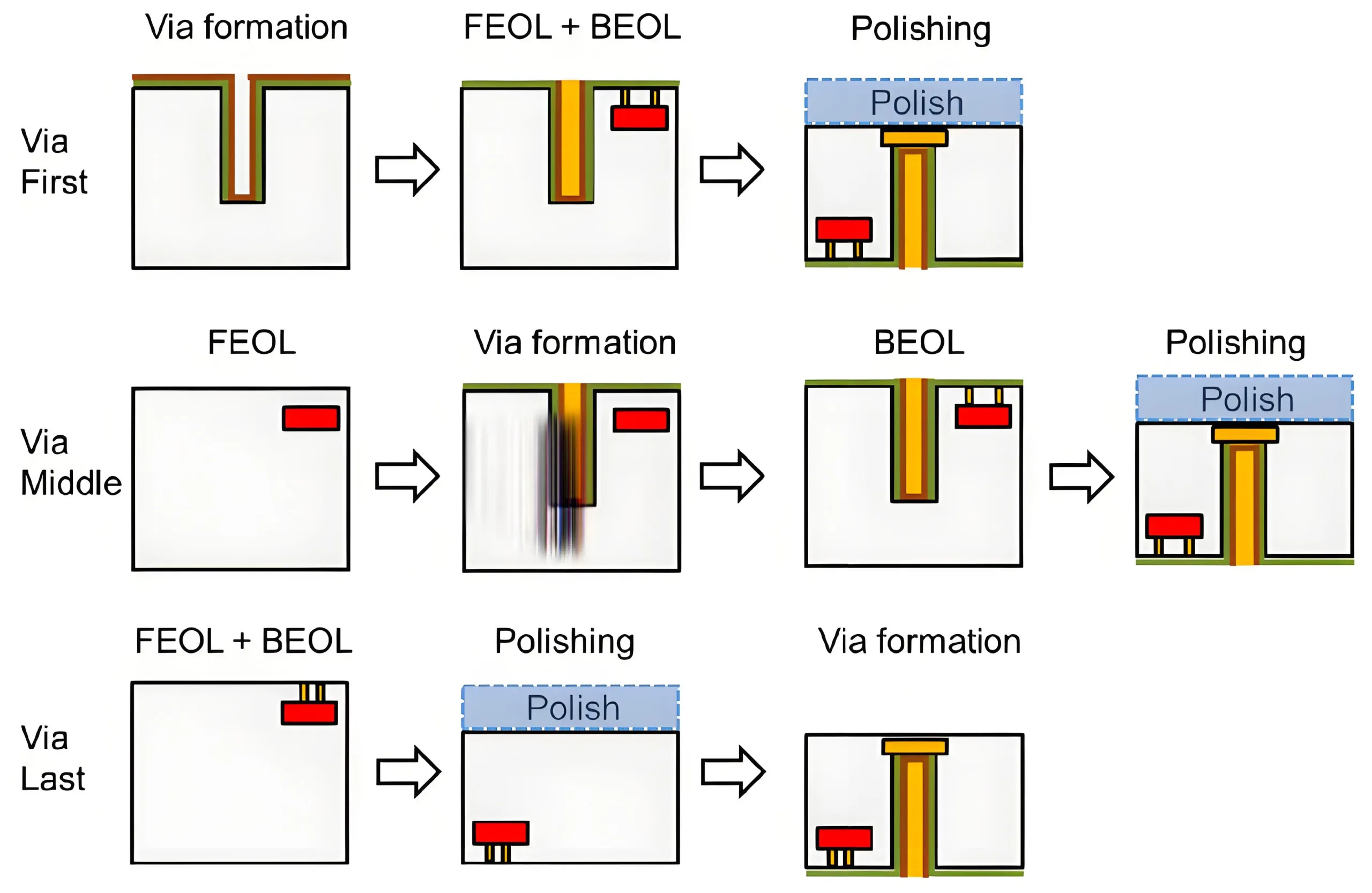
2. イノベーションを処理します: 工業化TGVテクノロジー
2.1 スルーグラスビア製造のブレークスルー
TitanRise Techのレーザー修正が達成されます 8,000 Vias/sec ±5μm精度 (3a), 160×従来の方法よりも高速. 重要な手順:
-
ピコ秒レーザー修飾: ミクロンスケールの変更ゾーンを作成します
-
HFエッチング: 達成 100:1 アスペクト比
-
金属化: PVDスパッタリング + 電気めっき (>15MPA接着)
2.2 金属化の進歩
4つの技術的ルートは、ガラスの接着に対応しています:
-
電気のない + マイクロエッチング (AKMソリューション)
-
ナノアグペースト + 焼結 (Wintech特許)
-
プラズマ移植 (IME-CASテクノロジー)
-
スタック付きPVD Ti/ (TitanRise標準)
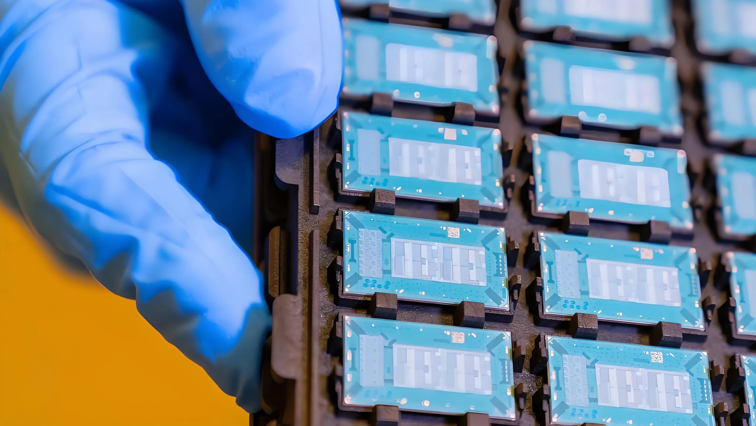
その中で, UGPCB DEP600機器の導入に多額の投資を行ってきました, 高アスペクト比スパッタリングテクノロジーを採用しています, 達成 95% カバレッジ 10:1 ホールプロファイル, 少ない金属抵抗率で 2.5 μω・cm, 国際的に主要なレベルに達する.
3. 産業環境: グローバルな競争が激化します
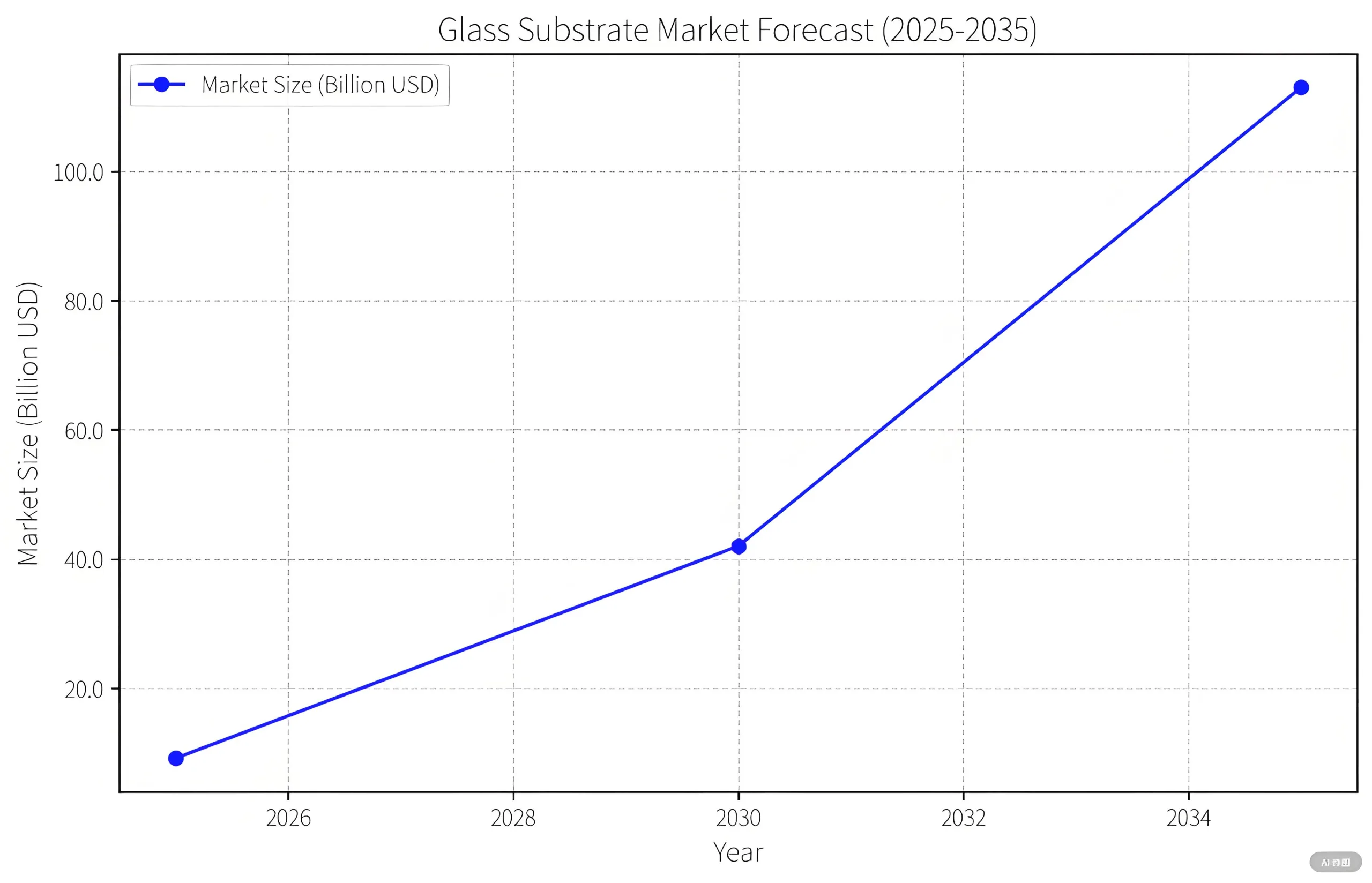
3.1 市場の成長予測
Prismarkは爆発的な拡大を予測しています:
-
2025: $916m (TGV基板)
-
2030: $4.2B (完全なアプリケーション)
-
2035: $11.3B (エコシステム全体)
3.2 地政学的な技術レース
-
アメリカ合衆国: Intel標準 + コーニング供給の支配
-
韓国: サムスンの “Glass Alliance” + SKCの9層スタック
-
中国: Wintech/AKM大量生産 + jfe 2026 ローカリゼーション
4. 課題 & ソリューション: 商業化のハードル
4.1 コスト削減経路
現在の3-5×コストプレミアム対従来の基質は急落します:
-
85% 大型パネル (>2m²) 利用
-
90% レーザー掘削コスト削減
-
金属化の収率改善 (60%→92%)
4.2 信頼性認証
新しい基準が必要です:
-
サーマルサイクリング (-55°C -250°C, 1,000 サイクル)
-
em lifetime (mttf >10hours @ jep154)
-
高周波安定性 (<0.5DB/CM @100GHz)
5. PCB業界への影響: 脅威対機会
5.1 市場の混乱
-
30% HDI/基板 交換リスク
-
ハイブリッド (ガラス+樹脂) 基板の機会
5.2 テクノロジーの相乗効果
-
ピコ秒レーザー掘削採用
-
PVD強化 HDI トレース精度
-
光学検査 <0.1μm解像度
結論: 透明な基質, 不透明な未来
現在、中国は重要なTGVセクターを率いています (装置, テスト, 材料). IntelのPat Gelsingerが指摘しているように: “物質的な革新は、原子スケールでの新しいムーアの法律になります。” このガラス駆動型革命は、半導体の2番目の成長曲線のロックを解除する可能性があります.
