
In the world of プリント基板設計, copper pour is a subtle art. It involves filling unused board areas with copper. This act is not merely aesthetic. It is a precise balance of signal integrity, 熱管理, and manufacturing efficiency. For a layout engineer, copper pour is not just drawing shapes. It is about finding the optimal point between circuit performance and design for manufacturability (DFM).
1. The Benefits: Building a Foundation for Performance
Copper pour is common in high-frequency and high-speed digital circuits. It is valued for its physical and electrical benefits.
あ. A Low-Impedance Shield
From an electromagnetic compatibility (EMC) perspective, copper pour’s main value isreducing ground impedance. Ohm’s Law states that impedance increases with length and decreases with cross-sectional area. Filling empty areas with solid copper, tied to the ground net, creates a low-impedance reference plane. This shortens signal return paths. It minimizes loop area. It also forms a Faraday cage-like shield, which suppresses common-mode radiation.
B. Efficiency Through Conductivity
In high-current designs, copper acts as a conductor. The IPC-2221 standard provides a formula for current-carrying capacity:
ここ, 私 is current in Amperes.dT is temperature rise in °C.あ is cross-sectional area in mil².k 補正係数です (0.024 for inner layers, 0.048 外層用). Increasing the copper pour area raisesあ. This allows more current at the same temperature rise. For power supplies, this reduces voltage drop (V=そして). It cuts energy loss and prevents hot spots. This is key for high-reliability プリント基板.
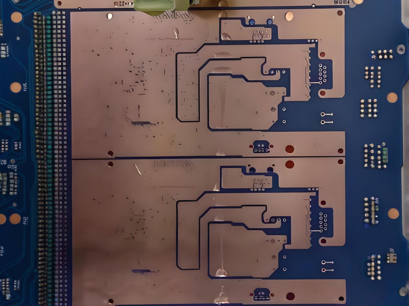
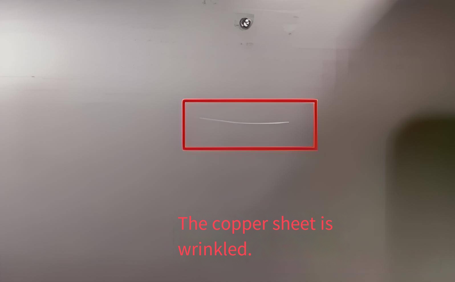
C. Mechanical Support During Lamination
During multilayer lamination, copper pour acts as a support structure. If inner layers have large empty areas, the prepreg (PP) resin flows unevenly. This happens under high temperature and pressure. The resin pools in copper-free zones. This leads to uneven board thickness. It can cause copper wrinkling, 剥離, or white spots.
2. The Risks: When Copper Pour Causes Problems
しかし, improper copper pour can create issues. It may turn from a solution into a source of EMI or manufacturing defects.
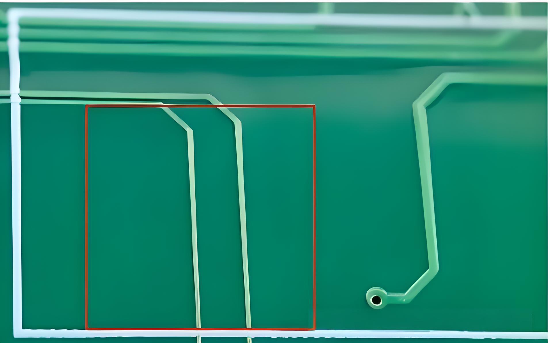
あ. The Antenna Effect of Copper Islands
On outer layers, copper planes are often split by components and traces. If isolated copper areas (copper islands) are not tied to the main ground plane with vias, they become floating conductors. Electromagnetic theory shows that floating conductors in a varying electric field can act asdipole antennas. They radiate EMI. Poorly grounded copper pour is worse than no copper pour at all. It creates hard-to-trace EMC failures.
B. Thermal Management Conflicts
During PCBA rework, large copper areas make soldering hard. Copper has high thermal conductivity, について400 w/(m⋅K). Large pours quickly absorb heat from soldering irons or hot air guns. This makes desoldering difficult. For hand-soldered parts or pads with hot air leveling (出血), thermal relief spokes (cross-shaped connections) are better. They slow heat transfer to the copper plane.
C. Manufacturing Defects: Dry Film Tenting
From a プリント基板 plating perspective, copper pour layout affects plating current uniformity.
During electroplating, exposed circuit patterns are plated. Faraday’s Law dictates that plating thickness is proportional to current density. If an isolated trace has low surrounding copper density, its current density rises. This causes excessive copper plating. The result is two defects:
- Pseudo-exposure: Solder mask becomes thin over over-plated traces, causing yellowing or exposed copper.
- Dry film tenting: When trace spacing is only 4-5 ミル, over-plating traps dry film between traces. This prevents etching, causing short circuits.
3. DFM Rules: Balancing Design and Process
Given these risks, what design rules should engineers follow? These guidelines, drawn from IPC-6012 (Rigid Printed Board Qualification) and manufacturing experience, help balance performance with yield.
あ. 内層: Pour for Lamination Control
For multilayer boards, inner-layer copper pour is crucial for resin flow balance. This is especially true under areas like gold fingers. If the inner layers under gold fingers are empty, the final board thickness will be thinner in that area. This causes poor contact with connectors. Inner-layer pour ensures thickness tolerance meets IPC Class 2 またはクラス 3 要件.
B. 外層: Pour for Plating Uniformity
Designers should avoid isolated traces on outer layers. If they are unavoidable, follow spacing rules based on copper weight:
- Copper weight ≤ 1 オンス: Minimum spacing should be at least 6 ミル.
- Copper weight ≥ 2 オンス: Minimum spacing should be at least 8 ミル.
These rules help dry film adhesion and prevent “tenting” issues.
C. Special Area Considerations
- Antenna Zones: In RF designs, copper pour must follow the chip vendor’s design guide. If dummy copper is used, it should be far from the antenna. It must connect to the ground plane with dedicated vias. This prevents parasitic capacitance from shifting the antenna’s resonant frequency.
- Board Edges and Mounting Holes: Keep copper at least 0.5 mm away from board edges and non-plated holes. This avoids shorts from routing or mechanical damage.
4. 結論: Finding the Optimal Balance
PCB copper pour is a balancing act. Good copper pour reduces ground impedance and improves EMC. It also balances plating current, raising PCBA yields. Poor copper pour creates EMI sources and manufacturing defects.
As a professional PCB and PCBAsupplier, we recommend early DFM collaboration. 必要な場合は、引用 for a high-density multilayer board, contact our engineering team. We provide design advice based on IPC標準 and real manufacturing data. Let us help you move from prototype to mass production with confidence.
Data and Formula References
- Current-Carrying Formula: Derived fromIPC-2221, Generic Standard on Printed Board Design. This is the industry standard for conductor capacity calculations.
- 熱伝導率: Pure copper’s thermal conductivity is cited as approximately400 w/(m⋅K), a standard physical value used in thermal management.
- Design Rules: Spacing recommendations (6 mil for 1 オンス, 8 mil for 2 オンス) align with DFM guidelines from leading PCB manufacturers to prevent “dry film tenting” and ensure reliable etching.
