

12L 2+N+2 HDI PCBとは?
12L 2+N+2 HDI PCB は 12 層を指します。 高密度相互接続 (HDI) プリント基板, N 個の信号層が隣接する 2 つのコア層と、別の 2 つのコア層を備えています。. この構成により、高密度の相互接続が可能になります。, 高度な電子アプリケーションに適したものになります. The “2+n+2” 名称はコア層と信号層の配置を示します.
設計上の考慮事項
12L 2+N+2 HDI PCB の設計には、いくつかの重要な要素が含まれます:
- レイヤースタッキング: 最適な電気的性能を確保するためのコア層と信号層の適切な配置.
- トレースとスペース: 微細なフィーチャに対応するための最小トレース幅と 3mil/3mil のスペース.
- 穴のサイズ: 最小 0.2 mm の機械穴と最小 0.1 mm のレーザー穴により、部品を正確に配置できます。.
- 銅の厚さ: 導電性と柔軟性のバランスをとるために、内層が 1OZ、外層が 0.5OZ のさまざまな銅厚.
それはどのように機能しますか?
12L 2+N+2 の機能 HDI PCB 多層構造と高密度相互接続の使用に依存. 各層は特定の目的を果たします:
- コア層: 構造的完全性を提供し、信号層の基盤として機能します.
- シグナルレイヤー: コンポーネント間で電気信号を伝送する.
- 表面処理: イマージョンゴールド + OSP により、酸化を防止することで優れたはんだ付け性と長期信頼性を確保.
アプリケーションと分類
 これら プリント基板 主に、コンパクトなサイズと高性能が重要なインテリジェントなデジタル製品で使用されます。. 複雑さとレイヤーの数に基づいて分類できます。, 12L 2+N+2 構成はさまざまな用途に非常に汎用性が高い.
材料とパフォーマンス
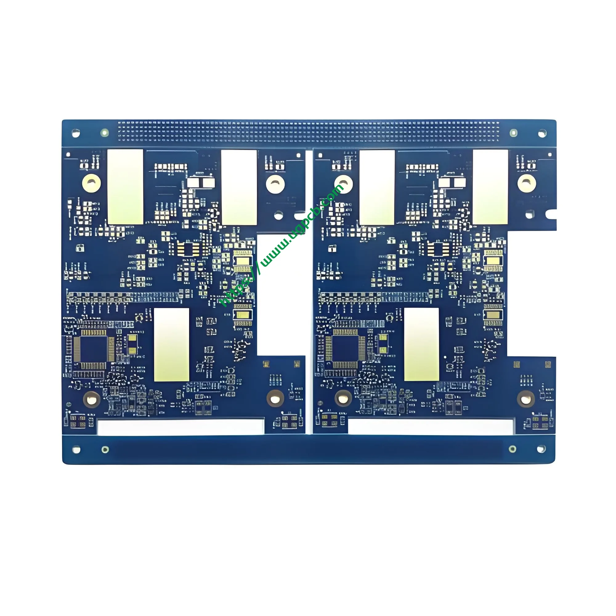
から構築 FR-4 アイテック, これらの PCB は優れた熱安定性と機械的強度を備えています. 青/白の配色は目視検査とトラブルシューティングに役立ちます. 仕上がりの厚さは 1.6 mm で、複雑なデザインに適した堅牢かつ柔軟な基板を提供します。.
構造と機能
12L 2+N+2 HDI PCB のユニークな構造には以下が含まれます。:
- 十二層: 2 つのコア層, n信号層, そして別の 2 つのコア層.
- 高密度相互接続: 複雑な配線と最小限のスペース使用を可能にします.
- 表面処理: 浸漬金と OSP が導電性を高め、腐食から保護します.
製造工程
製造プロセスにはいくつかの高度なステップが含まれます:
- 材料の準備: 高品質なFR-4基板と銅箔の選択.
- レイヤースタッキング: 目的を達成するためにレイヤーを正確な順序で配置する “2+n+2” 構成.
- ボンディング: 熱と圧力を使用して層を結合します.
- エッチング: 余分な銅を除去するためにエッチャントを適用します, 目的の導電性経路のみを残します.
- メッキ: 金属の薄い層を追加して、導電性とはんだ付け性を向上させます。.
- 表面処理: 浸漬金プラス OSP を適用して酸化を防ぎ、はんだ付け性を向上させます。.
- 品質管理: 各ボードが厳しい品質基準を満たすように徹底的な検査とテストを実施する.

ユースケースとシナリオ
12L 2+N+2 HDI PCB は、小型化と高性能が重要なインテリジェント デジタル製品での使用に最適です. 一般的なアプリケーションには含まれます:
- スマートフォン: 機能やパフォーマンスを損なうことなく、よりスリムなデザインを有効にします.
- タブレット: 高速データ転送と処理のための信頼できる接続を提供します.
- ウェアラブルデバイス: 堅牢なパフォーマンスと耐久性を維持しながら、コンパクトなデザインをサポートします.
- ポータブルメディアプレーヤー: 小さなフォームファクターで高品質のオーディオおよびビデオ処理機能を確保する.
結論は, 12L 2+N+2 HDI PCB は PCB テクノロジーの革新の頂点を表します, 比類のない密度を提供します, パフォーマンス, 最も要求の厳しい消費者電子アプリケーションの信頼性.


