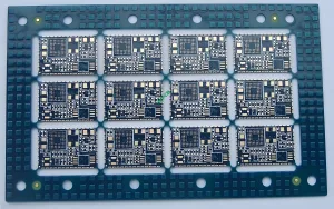
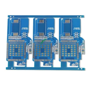
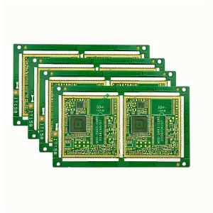
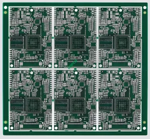
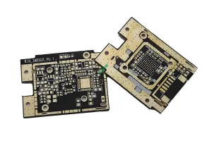
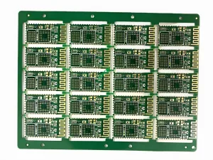
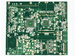
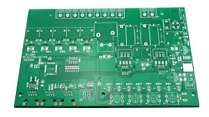
の紹介 6 レイヤーPCB
The 6 Layer PCB is a sophisticated 電子部品 designed for high-performance applications requiring complex circuitry. It consists of six layers of conductive material, 通常は銅, 絶縁層によって分離されています. This multilayer structure allows for greater functionality and compactness compared to single or 両面PCB.
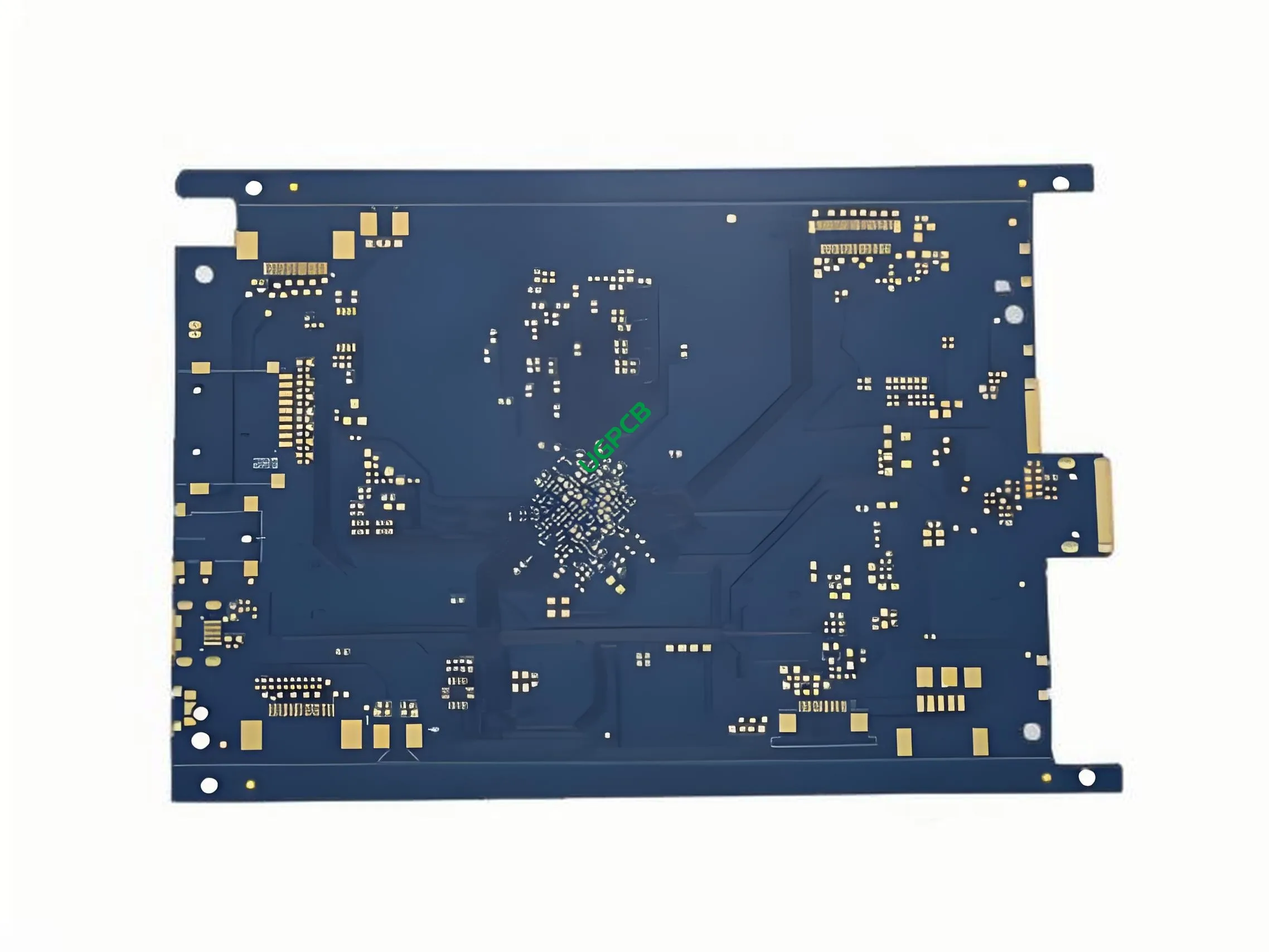
何ですか 6 レイヤーPCB?
あ 6 レイヤーPCB, または プリント基板, is an advanced electronic substrate that features six layers of conductive pathways embedded within insulating layers. These layers are meticulously arranged to create intricate circuit designs suitable for demanding electronic applications. The additional layers provide enhanced signal integrity, 配電, and thermal management capabilities.
設計要件
Designing a 6 Layer PCB involves several critical considerations:
- 材料の選択: Common materials include S1141, S1000, そして 370人事部, chosen based on their electrical properties and compatibility with the manufacturing process.
- レイヤーのスタックアップ: Determines the arrangement of signal and ground planes, crucial for minimizing crosstalk and ensuring reliable signal transmission.
- 銅の厚さ: Typically specified as 1/H/H/H/H1 OZ, indicating varying thicknesses across different layers to optimize performance and cost.
- 表面処理: Options like Immersion Gold or OSP (Organo-Silicon Protection) are applied to protect the copper surfaces and enhance solderability.
仕組み?
The 6 Layer PCB functions by providing a platform for electrical components to be interconnected through a series of conductive paths etched onto its surface. Each layer contains specific patterns of copper traces that form circuits when connected via plated through-holes or vias. The multiple layers enable more complex circuit designs without increasing the board’s footprint, making it ideal for modern electronic devices where space is limited.
アプリケーション
Due to their complexity and capability to handle high-speed signals with minimal interference, 6 Layer PCBs are widely used in consumer electronics such as smartphones, 錠剤, ラップトップ, その他のポータブルデバイス. They are also found in automotive electronics, 医療機器, and industrial controls where reliability and performance are paramount.

分類
6 Layer PCBs can be classified based on several factors:
- 素材によって: As mentioned, they may use S1141, S1000, or 370HR depending on the required characteristics.
- アプリケーションによって: General-purpose or specialized for specific industries like telecommunications, 航空宇宙, or defense.
- 表面処理による: Different finishes like Immersion Gold or OSP cater to various environmental conditions and soldering processes.
使用材料
The primary materials used in manufacturing 6 Layer PCBs include:
- 基本材料: Often fiberglass-reinforced epoxy resins (FR-4), which offer excellent mechanical strength and thermal stability.
- 銅箔: Varying thicknesses are used to balance conductivity and cost-effectiveness.
- はんだマスク: Typically green in color, 銅配線を酸化や偶発的な短絡から保護します。.
- シルクスクリーン: A white coating used for labeling components and providing instructions for assembly.
性能特性
Key performance attributes of a 6 Layer PCB include:
- 信号の完全性: Enhanced by strategic layer placement and grounding schemes.
- 熱管理: Improved heat dissipation due to larger copper areas and potentially thicker boards.
- 機械的強度: Multilayer construction adds rigidity, reducing the risk of damage during handling or operation.
構造組成
構造的に, a 6 Layer PCB comprises:
- 導電層: Six layers of copper traces separated by dielectric materials.
- 絶縁層: 導電層間の電気的短絡を防止.
- ビア: Conductive holes that connect different layers, allowing vertical integration of circuits.
特徴的な機能
Some notable features of a 6 Layer PCB are:
- 高密度: Allows for complex circuit designs within a compact form factor.
- 信頼性: Multilayer design improves resistance to electromagnetic interference (エミ).
- 多用途性: Suitable for a wide range of applications due to customizable layer configurations and material choices.
製造工程
The manufacturing process of a 6 Layer PCB involves several steps:
- デザインとレイアウト: 専用ソフトを使って回路パターンを作成.
- 材料の準備: 基材をサイズに合わせて切断し、表面を洗浄します.
- ラミネート加工: 熱と圧力の下で個々の層を積み重ねて接着する.
- エッチング: 余分な銅を除去して目的の回路経路を形成する.
- メッキ: ビアと露出した銅領域に金属の薄い層を追加する.
- ソルダーマスクの塗布: Applying the green coating to protect traces.
- シルクスクリーン印刷: Adding text and symbols for component placement.
- 最終検査: 出荷前に品質と機能を保証する.
ユースケース
Common scenarios where a 6 Layer PCB might be employed include:
- モバイルデバイスの高密度相互接続アプリケーション.
- 低信号損失を必要とする高度な通信システム.
- 過酷な環境でも信頼性の高い性能を必要とするポータブル医療機器.
- 堅牢性と長寿命が求められる自動車エレクトロニクス.
要約すれば, の 6 Layer PCB represents a significant advancement in printed circuit board technology, 最新の電子アプリケーションに比類のない複雑さとパフォーマンスを提供します. 設計の柔軟性, 優れた信号整合性と耐久性を兼ね備えています, makes it an essential component in the development of next-generation consumer electronics and beyond.