

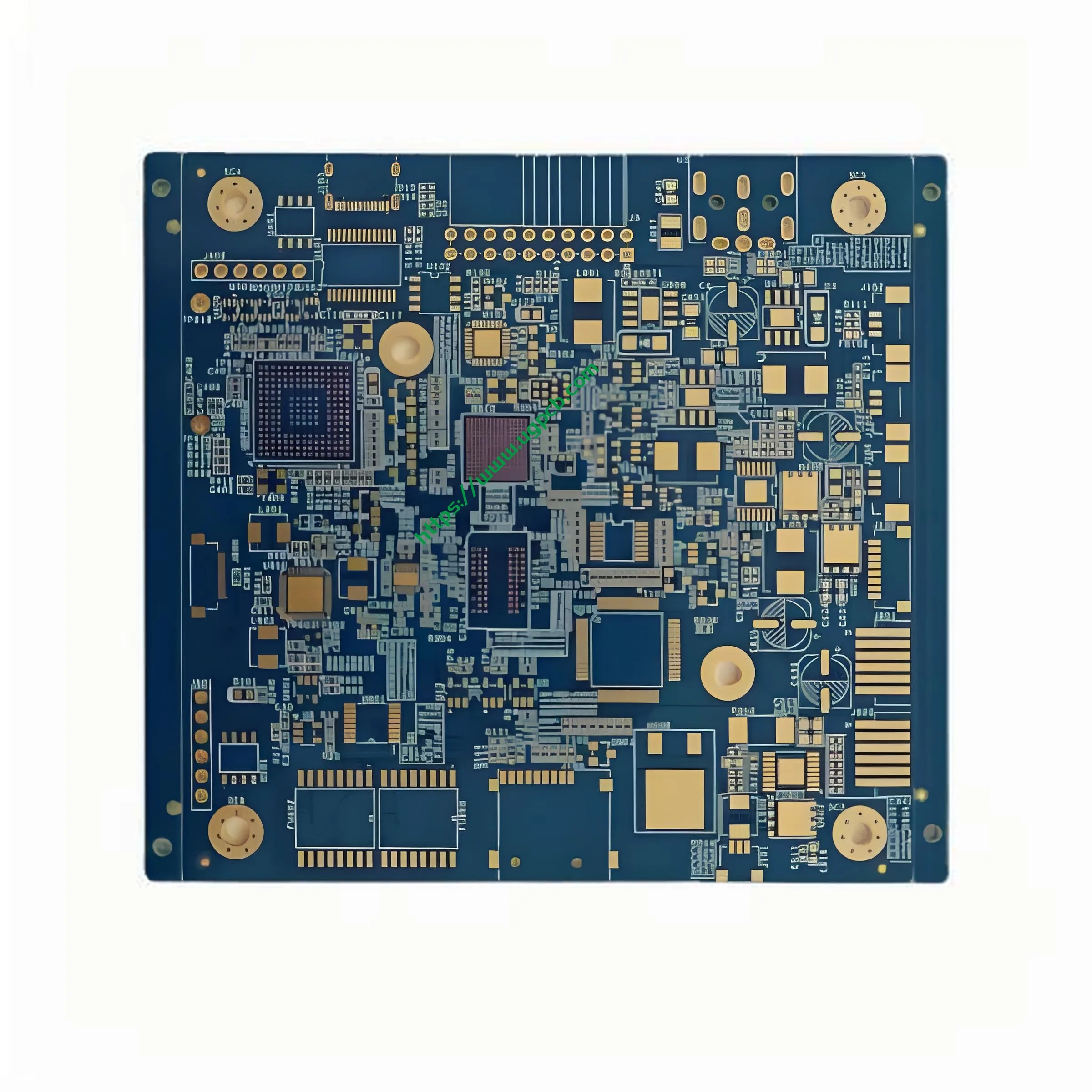
What is a 6L 1+N+1 HDI PCB?
A 6L 1+N+1 HDI PCB stands for a six-layer High Density Interconnect (HDI) プリント基板, featuring one core layer flanked by N signal layers and another core layer. この構成により、高密度の相互接続が可能になります。, 高度な電子アプリケーションに適したものになります. The “1+n+1” designation refers to the arrangement of the core layers and signal layers.
設計要件
The design of a 6L 1+N+1 HDI PCB requires careful consideration of several factors:
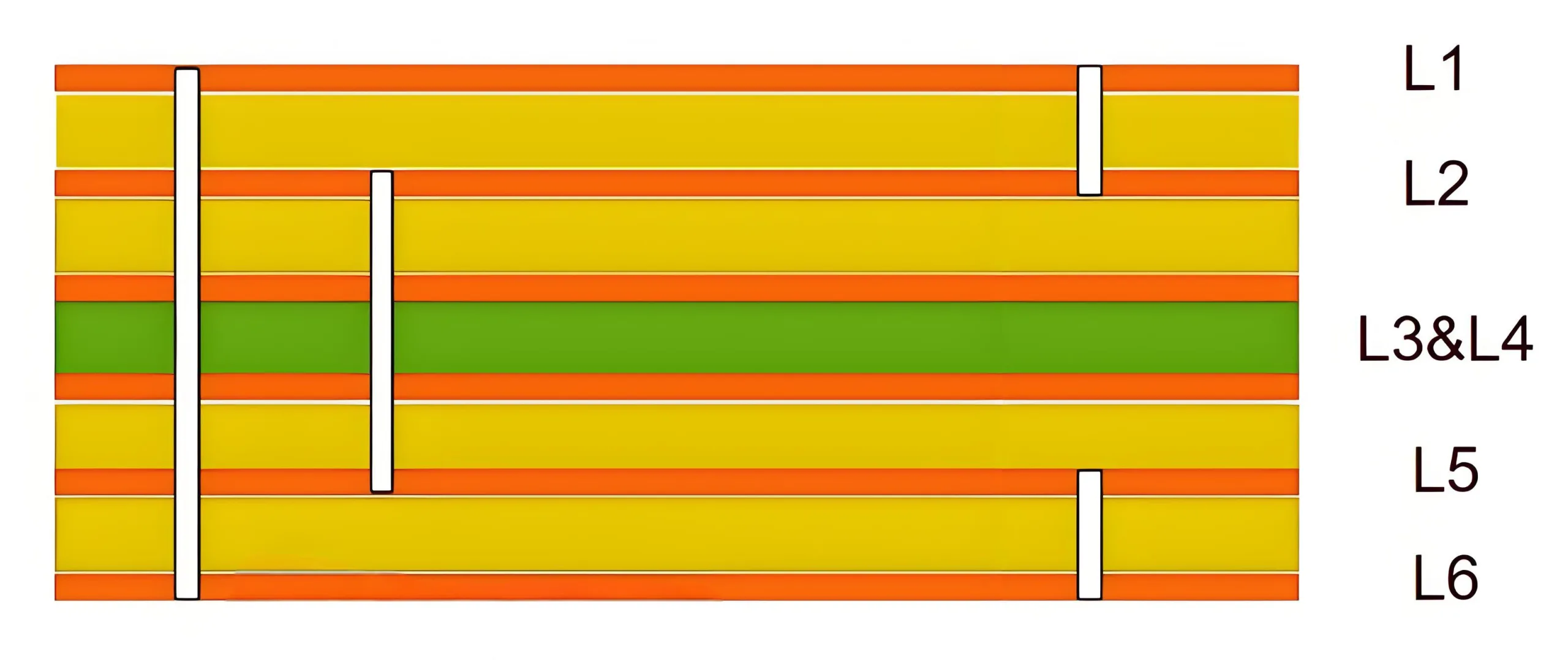
- レイヤースタッキング: 最適な電気的性能を確保するためのコア層と信号層の適切な配置.
- トレースとスペース: 微細なフィーチャに対応するための最小トレース幅と 3mil/3mil のスペース.
- 穴のサイズ: 最小 0.2 mm の機械穴と最小 0.1 mm のレーザー穴により、部品を正確に配置できます。.
- 銅の厚さ: 導電性と柔軟性のバランスをとるために、内層が 1OZ、外層が 0.5OZ のさまざまな銅厚.
それはどのように機能しますか?
The functionality of a 6L 1+N+1 HDI PCB 多層構造と高密度相互接続の使用に依存. 各層は特定の目的を果たします:
- コア層: 構造的完全性を提供し、信号層の基盤として機能します.
- シグナルレイヤー: コンポーネント間で電気信号を伝送する.
- 浸漬金表面処理: Ensures excellent solderability and long-term reliability by preventing oxidation.
アプリケーションと分類
これら プリント基板 主に、コンパクトなサイズと高性能が重要なインテリジェントなデジタル製品で使用されます。. 複雑さとレイヤーの数に基づいて分類できます。, with the 6L 1+N+1 configuration being highly versatile for various applications.
材料とパフォーマンス
から構築 FR-4 (ITEQ), これらの PCB は優れた熱安定性と機械的強度を備えています. 緑/白の配色は、目視検査とトラブルシューティングに役立ちます. The finished thickness of 1.0mm provides a robust yet flexible board suitable for intricate designs.
構造と機能
The unique structure of a 6L 1+N+1 HDI PCB includes:
- Six Layers: One core layer, n信号層, and another core layer.
- 高密度相互接続: 複雑な配線と最小限のスペース使用を可能にします.
- 浸漬金表面: Enhances conductivity and protects against corrosion.
製造工程
製造プロセスにはいくつかの高度なステップが含まれます:
- 材料の準備: 高品質なFR-4基板と銅箔の選択.
- レイヤースタッキング: 目的を達成するためにレイヤーを正確な順序で配置する “1+n+1” 構成.
- ボンディング: 熱と圧力を使用して層を結合します.
- エッチング: 余分な銅を除去するためにエッチャントを適用します, 目的の導電性経路のみを残します.
- メッキ: 金属の薄い層を追加して、導電性とはんだ付け性を向上させます。.
- 表面処理: Applying immersion gold to protect against oxidation and enhance solderability.
- 品質管理: 各ボードが厳しい品質基準を満たすように徹底的な検査とテストを実施する.

ユースケースとシナリオ
6L 1+N+1 HDI PCBs are ideal for use in intelligent digital products where miniaturization and high performance are critical. 一般的なアプリケーションには含まれます:
- スマートフォン: 機能やパフォーマンスを損なうことなく、よりスリムなデザインを有効にします.
- タブレット: 高速データ転送と処理のための信頼できる接続を提供します.
- ウェアラブルデバイス: 堅牢なパフォーマンスと耐久性を維持しながら、コンパクトなデザインをサポートします.


