

1. 製品の概要
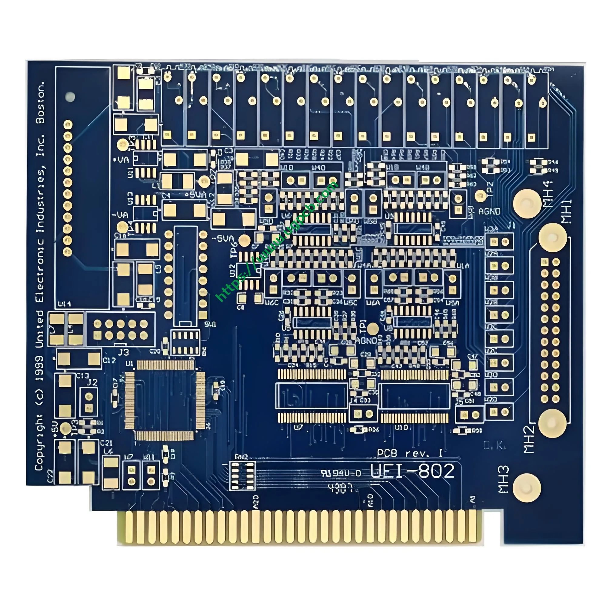
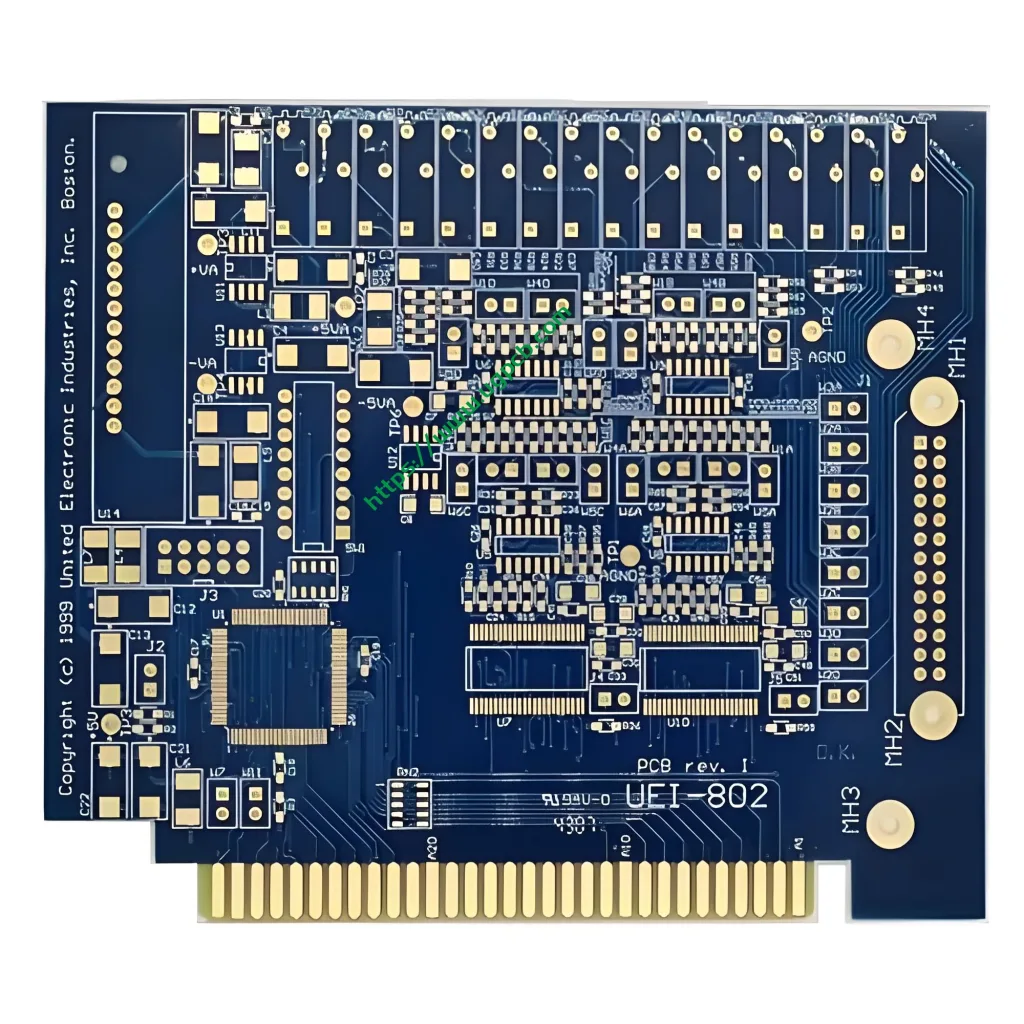
両面ゴールドフィンガー プリント基板 (プリント基板) 一般に「ゴールドフィンガー」と呼ばれる金メッキ接点が基板の端に沿って配置されているのが特徴です. これらのコンタクトは、相手コネクタに挿入されると、プラグ可能な電気経路を作成します。, カードスロットやソケットなど. すべての信号と電力はこれらのフィンガー型端子を介して流れます。.
UGPCB の両面ゴールドフィンガー PCB は 2 層設計の FR4 基板を使用しています. 板厚は、 1.6 mm, 内層と外層の両方に 1 oz銅. ドリルビアの最小直径は次のとおりです。 0.3 mm, トレースの幅と間隔は両方とも 0.15 mm. 表面仕上げはイマージョンゴールドです (同意する) ボード全体にわたって, 追加の電気めっきハードゴールドをゴールドフィンガー領域に選択的に適用. この製品は、ゴールドフィンガー接続の実証済みの信頼性とともに、両面ボードの配線の柔軟性を提供します。. 基板間プラグインインターフェイスを必要とする幅広い電子システムに対応します。.
2. 製品の分類と位置付け
IPC‑6012に準拠 (リジッドプリント基板の認定および性能仕様), この製品は次のカテゴリに分類されます:
| 分類次元 | カテゴリ |
|---|---|
| 構造によって | 両面 PCB – 両面の導電性トレース |
| 相互接続方式別 | メッキスルーホール付き (PTH) |
| IPC‑6012 パフォーマンスクラスによる | クラス 2 (専用サービスの電子製品) – ほとんどのゴールドフィンガー用途に適しています |
| 基板材質別 | FR4硬質ラミネート (S1141グレード) |
| 表面仕上げによる | 同意する (無電解ニッケル / 浸漬ゴールド) + ゴールドフィンガーに選択的に電気メッキされたハードゴールド |
| 機能別 | ゴールドフィンガーPCB / エッジコネクタPCB |
この製品は、中~高信頼性のプラグイン接続 解決. 両面配線の自由な設計とゴールド フィンガー エッジ コネクタの信号整合性を組み合わせます。.
3. 主要な技術的パラメータ
3.1 基板: FR4 + S1141 ラミネート
FR4 は PCB 業界で最も一般的なリジッド基板です. ガラス繊維強化エポキシ樹脂で構成されています, 優れた機械的強度を提供します, 電気断熱, および熱抵抗. この製品が使用しているのは、 S1141 FR4 ラミネート Shengyi Technology より, IPC‑4101/21に準拠.
S1141 の主要業績評価指標 (でテストされました 1.6 mm試験片) 以下にリストされています.
| パラメーター | 代表値 | テスト方法 |
|---|---|---|
| ガラス転移温度 (TG) | 140℃ (DSC) | IPC-TM-650 2.4.25 |
| 熱分解温度 (TD) | 310℃ (5 % 減量) | IPC-TM-650 2.4.24.6 |
| Z 軸 CTE (tgの前) | 65 ppm/°C | IPC-TM-650 2.4.24 |
| Z 軸 CTE (Tg後) | 300 ppm/°C | IPC-TM-650 2.4.24 |
| 誘電率 (DK, 1 MHz) | 4.6 | IPC-TM-650 2.5.5.9 |
| 損失係数 (Df, 1 MHz) | 0.015 | IPC-TM-650 2.5.5.9 |
| 可燃性評価 | UL 94 V-0 | UL 94 |
| 吸水性 | 0.15 % | IPC-TM-650 2.6.2.1 |
データソース: Shengyi S1141 技術データシート, IPC‑4101/21に準拠.
UL 94 V-0 UL で最高の難燃性評価です 94 垂直燃焼試験. 10秒間の炎を2回当てた後、, 各試験片の総燃焼時間が超えないこと 10 秒, 炎の滴が綿インジケーターに点火することはありません. これにより、異常な加熱や短絡状態でも PCB が安全に保たれます。.

3.2 板厚: 1.6 mm
The 1.6 mm の厚さはリジッド PCB の業界標準です. S1141 材料特性データのベースライン厚さとしても機能します。. この厚さにより、機械的強度との最適なバランスが実現されます。, 挿入安定性, そして製造コスト. 標準コネクタスロットと幅広く互換性があります.
3.3 銅の厚さ: 1 オンス (約 35 μm)
内層銅箔、外層銅箔とも1 オンス (オンス) , これはおよそ 35 厚さμm. IPC‑6012に準拠, クラスの最小仕上げ銅厚さ 1 とクラス 2 ボードは 48 μm. から始まる 1 オンスの箔は、加工後の最終的な厚さがこれらの要件を満たすことを保証します。. この銅製の重りは適切な通電容量をサポートします (約4~6A, トレース幅に応じて) ファインラインのエッチング精度を維持しながら. トレースの幅と間隔 0.15 mm (について 6 ミル) 確実に生産可能です 1 oz銅.
3.4 最小ビア直径: 0.3 mm
機械的に開けられる最小の穴の直径は次のとおりです。 0.3 mm, これは標準的なスルーホール技術の能力の範囲内に十分収まります. メッキスルーホール対応 (PTH) 層間で信頼性の高い電気的相互接続を確保するための処理. IPC-6012の場合, すべての PTH は熱ストレス試験に合格する必要があります (288 ℃はんだディップ) 構造の完全性を検証するため.
3.5 トレース幅と間隔: 0.15 mm / 0.15 mm
トレース幅 0.15 mm (約 6 ミル) と間隔 0.15 mm は従来の PCB 製造におけるファインライン能力を表します. で 1 OZ銅の厚さ, a 0.15 IPC-2221 の計算に基づくと、mm トレースは約 0.5 ~ 0.8 A の電流を流すことができます。. これにより、ほとんどの信号伝送および低電力供給アプリケーションのニーズが満たされます。. この幅と間隔の組み合わせにより、製造コストを抑えながら信頼性が確保されます。.
4. 表面仕上げ: イマージョンゴールドと電気メッキゴールドフィンガー
この製品には、複合表面仕上げプロセス: 浸漬ゴールド (同意する) 全体的に, と電気メッキされたハードゴールド ゴールドフィンガー領域に選択的に適用されます. これはゴールドフィンガー PCB の標準かつ最適なプロセスです.
4.1 イマージョンゴールド (同意する) プロセス
無電解ニッケル / イマージョンゴールド (同意する) 最初にニッケルを銅の表面に化学的に堆積させる仕上げです。, 続いて、置換反応によって薄い金の層が堆積されます。.
あたりIPC‑4552 リビジョン A (発行済み 2017) :
- ニッケルの厚さ: 3 μmから 6 μm (120 μinから 240 分)
- 金の厚さ: 0.04 μmから 0.10 μm (1.6 μinから 4.0 分)
- 推奨される金の厚さ: 0.04 μmから 0.07 μm (1.6 μinから 2.8 分)
データソース: IPC‑4552 – 無電解ニッケルの性能仕様 / イマージョンゴールド (同意する) プリント基板用めっき.
ENIGの利点:
- ファインピッチ配線やBGAパッケージに適した平坦な表面
- 鉛フリーはんだ対応に優れたはんだ付け性 (例えば。, SAC305)
- 強い酸化耐性と長い保存寿命
- 薄い金層でコストを管理可能
4.2 電気メッキされたゴールドフィンガー – 主要な特徴
ゴールドフィンガーエリアは、追加の電気メッキハードゴールド. ENIGで使用されるソフトゴールドとは異なります。, 電気メッキされたハードゴールド コバルトやニッケルなどの硬化剤が含まれています (金コバルトまたは金ニッケル合金). その硬度はHVを超える可能性があります 200, ソフトゴールドよりもはるかに優れた耐摩耗性を実現.
なぜゴールドフィンガーには電気メッキされたハードゴールドを使用しなければならないのか?
ENIGゴールドは非常に薄いです (わずか0.04~0.10μm) そして柔らかい (HV以下の硬度 90). わずか 3 ~ 5 回の挿入サイクルで摩耗します。. 電気メッキされたハードゴールド, 通常以上の厚さ 0.76 μm, 数百回または数千回の挿入サイクルに耐えることができます.
あたりIPC‑4556 (ハードゴールドの性能仕様) :
| アプリケーションクラス | 最小の金の厚さ | 典型的なアプリケーション |
|---|---|---|
| クラス 2 (耐久性のある) | ≥ 0.76 μm (30 分) | ほとんどのゴールドフィンガーアプリケーション |
| クラス 3 (高い信頼性) | ≥ 1.27 μm (50 分) | 高サイクル挿入, 工業用 / 軍隊 |
| ニッケル下地層 | 3‑5μm | すべてのハードゴールド預金に必要です |
データソース: IPC‑4556 – コネクタおよびゴールドフィンガー用の電気めっきハードゴールドの性能仕様.
この製品に使用されている電気メッキゴールドフィンガープロセスは、IPC‑4556クラスに準拠しています。 2 授業を通して 3 標準, 挿入寿命と接触信頼性の確保.
5. 設計上の考慮事項
5.1 ゴールドフィンガー面取り
ゴールドフィンガーの挿入端は、面取りされた コネクタスロットへのスムーズな挿入を可能にする.
- 面取り角度: 通常は 30° または 45°
- 面取り深さ: のために 1.6 板厚mm, 面取りの深さは通常 0.8 ~ 1.0 mm です。, 先端に 0.6 ~ 0.8 mm の鈍いエッジを残す
- チップ残り厚さ: 元の板厚の約1/3~1/2
- 重要な要件: 面取り領域をソルダーマスクで覆うことはできません, 金の層は面取りされたベベルを完全に覆う必要があります
5.2 ゴールドフィンガー領域の設計ルール
- ゴールドフィンガーはボードの端に整然と配置される必要があります
- 隣接するゴールドフィンガー間の最小間隔は ≥ である必要があります。 7 ミル (約 0.178 mm)
- ゴールドフィンガー領域は、明示的なめっき指示とともにガーバーファイルに明確にマークされている必要があります
5.3 インピーダンス制御の考慮事項
FR4 材料の誘電率 Dk = 4.6 で 1 MHz. のために 50 Ω シングルエンドまたは 100 Ω 差動インピーダンス制御, 設計者はトレース幅と誘電体の厚さを調整可能. The 0.15 この製品のトレース幅と間隔は mm で、標準設計のシグナル インテグリティ要件のほとんどを満たしています。.
6. 作業原則
両面ゴールドフィンガー PCB は 2 つのコアメカニズムを通じて動作します: 電気接点 そして信号伝送.
- 電気接続: 基板端のゴールドフィンガーコンタクトは、コネクタスロット内の金属スプリングコンタクトと物理的に嵌合します。, 低抵抗の電気経路の確立.
- 信号伝送: PCB はさまざまな信号からのルート信号をトレースします。 コンポーネント (チップ, 抵抗器, コンデンサ, 等) ゴールドフィンガーコンタクトへ, その後、コネクタを介してマザーボードまたはバックプレーンに送信されます。. 両面設計により、配線が可能 上層と下層の両方, 配線密度と設計の柔軟性が大幅に向上.
- プラグイン可能性: ゴールドフィンガー上の電気メッキされた硬質金層は、接触抵抗や信号の完全性を低下させることなく、複数回の挿入サイクルをサポートするのに十分な耐摩耗性を提供します。.
7. アプリケーションとユースケース
両面ゴールドフィンガー PCB は、必要な電子デバイスで広く使用されています。プラグ可能な接続. 一般的なアプリケーションには含まれます:
| 応用分野 | 特定の製品 |
|---|---|
| コンピューティング & サーバー | メモリモジュール (DDR, DDR2, DDR3, DDR4, DDR5), グラフィックカード, ネットワークインターフェースカード, 拡張カード |
| 家電 | USBドライブ, メモリーカード, カードリーダー, スマートフォン, スマートウォッチ |
| 通信機器 | ルーター, スイッチ, 通信モジュール |
| 産業管理 | 産業用制御ボード, データ収集カード, テストフィクスチャ |
| カーエレクトロニクス | 車載制御ユニット, インフォテインメントシステム |
| 医療機器 | 医療用電子モジュール (IPC‑6012EM医療サプリメントを使用) |
| 航空宇宙 | アビオニクスモジュール (IPC‑6012FS 航空宇宙サプリメント付き) |
FR4 両面ゴールドフィンガー PCB は、以下の用途に特に適しています。中程度の複雑さ, コスト重視のアプリケーション プラグイン接続が必要な場合.
8. 製造工程の流れ
UGPCB は、両面ゴールドフィンガー PCB の標準的な生産シーケンスに従います。:
- 切断 – FR4 銅張積層板を作業パネルの寸法に合わせて切断します.
- 掘削 – ドリル 0.3 mmの貫通穴と取り付け穴.
- PTH / パネルメッキ – 穴に無電解銅めっきを適用, 次にパネルプレート.
- パターン転写 – 回路パターンの露光と現像.
- パターンメッキ – 回路と穴を電解メッキして、 1 oz銅.
- エッチング – 保護されていない銅箔を除去して、最終的な回路トレースを形成します.
- はんだマスク – 緑色または他の色のソルダーマスクインクを塗布します.
- 表面仕上げ – ENIG – 無電解ニッケルと浸漬金を基板全体に塗布します.
- ゴールドフィンガーメッキ – ゴールドフィンガー領域にハードゴールドを選択的に電気めっきします.
- ゴールドフィンガー面取り – 挿入端の面取り.
- 電気試験 - 実行する 飛行探査機 または治具テスト.
- 目視検査 – IPC‑A-600に準拠した検査.
- パッキング & 配送 – 湿気を防ぐための真空パック.
9. 性能と品質の基準
この製品は、以下の国際規格に厳密に従って設計および製造されています。:
| 標準 | タイトル | 範囲 |
|---|---|---|
| IPC‑6012 | リジッドプリント基板の認定および性能仕様 | 全体的なパフォーマンスと信頼性 |
| IPC-A-600 | プリント基板の適合性 | 外観と合格基準 |
| IPC‑4552 | ENIG パフォーマンス仕様 | 浸漬金プロセス制御 |
| IPC‑4556 | 電気めっきハードゴールドの性能仕様 | ゴールドフィンガーハードゴールド加工 |
| IPC‑4101/21 | リジッドおよび多層プリント基板材料の仕様 | FR4材質仕様 |
| UL 94 V-0 | 安全性の基準 - プラスチック材料の可燃性 | 難燃認定 |
10. UGPCBを選択する理由?
- プロのゴールドフィンガー製造経験 – UGPCB は電気めっきと面取りにおいて成熟した機能を備えています.
- エンドツーエンドの品質管理 – 切断から最終検査までのすべてのステップが IPC 基準に従って管理されます.
- トレーサブルな材料 – 明確なソーストレーサビリティを備えた Shengyi S1141 などのブランド名 FR4 ラミネートを使用.
- 短納期 – 専用の両面 PCB 生産ラインが迅速なプロトタイピングと量産をサポート.
- テクニカルサポート – DFM を提供します (製造可能性のための設計) レビューとインピーダンス制御の推奨事項.
11. 今すぐ問い合わせる
UGPCB は、高価値の両面ゴールドフィンガー PCB ソリューションを世界中の顧客に提供することに尽力しています。. 必要かどうかサンプルプロトタイピング, 小ロット試作, または大量生産, 私たちはあなたにサービスを提供する専門知識を持っています.
見積もりについてはお問い合わせください:
- ガーバー ファイルを提供するか、 プリント基板設計 データ
- ゴールドフィンガーメッキの厚さを指定してください (0.76 μmから 1.27 μm推奨)
- 面取り角度の確認 (30°または45°) およびその他の特別な要件
データソース宣言
この文書の技術データと標準参考資料の出典は次のとおりです。: リジッドプリント基板の IPC‑6012 認定および性能仕様; 無電解ニッケルの IPC‑4552 性能仕様 / イマージョンゴールド (同意する) プリント基板用めっき; コネクタおよびゴールドフィンガー用の電気めっきハードゴールドの IPC‑4556 性能仕様; IPC-A-600 プリント基板の許容性; UL 94 安全性の基準 - プラスチック材料の可燃性; および Shengyi S1141 技術データシート (IPC‑4101/21に準拠).













