


私. 製品の概要
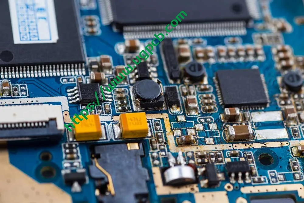
UGPCB 両面スルーホール PCB ボードは、高性能 2 層リジッド基板です プリント基板 FR-4 ガラスエポキシ基板上にメッキスルーホールを使用して構築 (PTH) テクノロジー. ボードの対策 86.9 × 73.58 厚さ mm 1.0 mm, 銅箔の厚さ 1/1 オズ (35 外層、内層ともにμm), 鉛フリー熱風はんだレベリング (出血) 表面仕上げ. ソルダーマスクは緑色です, そしてシルクスクリーンの伝説は白です.
両面スルーホール基板 (両面プリント基板) 絶縁基板の両面に導電性回路を備えています, 2 つの層間の電気的相互接続を可能にするメッキスルーホール付き. 片面 PCB との比較, 両面 PCB は 60% ~ 80% 高い配線密度を提供し、より複雑な回路設計をサポートします. UGPCB, ISO認定の品質システムとIPC準拠の製造プロセスによって裏付けられています, 高品質の両面スルーホール PCB とターンキーを提供します プリント基板 世界中の電子機器メーカーへのサービス.
Ⅱ. 製品定義と技術仕様
IPC-6012F による リジッドプリント基板の認定および性能仕様 (9月発行 2023), 両面スルーホール PCB は、メッキスルーホールを備えたリジッドプリント基板として分類されます。 (タイプ 2). その中心的な特徴は、銅メッキの穴壁を介した両側の導体間の電気接続です。. UGPCB は、IPC-6012F に完全準拠してこの製品を製造し、クラスを満たしています 2 パフォーマンス要件 (専用サービス用電子機器).
主な仕様:
| パラメーター | 仕様 |
|---|---|
| 基板材料 | FR-4 (難燃性UL 94 V-0) |
| レイヤー数 | 2 レイヤー (両面) |
| 板厚 | 1.0 mm |
| 基板寸法 | 86.9 × 73.58 mm |
| 最小穴の直径 | 0.236 mm |
| 最小線幅 / 間隔 | 0.32 × 0.37 mm |
| 銅箔の厚さ | 1/1 オズ (約. 35 各辺μm) |
| 表面仕上げ | 鉛フリーHASL (熱気はんだレベリング) |
| はんだマスク / 伝説 | 緑色のソルダーマスク / 白いシルクスクリーン |
Ⅲ. 設計ガイドライン
3.1 基板材料の選択 ― FR-4の工学的価値
FR-4 米国電気製造業者協会によって定められた難燃グレードの指定です。 (ありません). 文字 “フランス” 難燃剤の略, そしてその番号 “4” ガラス織布で強化されたエポキシ樹脂システムを示します. IPC-4101の場合 リジッド・多層プリント基板用基材仕様, FR-4 グレード A1 は、最適な機械的強度を備えたコア性能層を表します。, 電気的特性, そして長期的な信頼性.
FR-4の主要業績評価指標 (ソース: IPC-4101 および業界標準):
-
ガラス転移温度 (TG): 130–140℃ (標準FR-4)
-
誘電率 (DK) @ 1 GHz: 4.2-4.5
-
損失係数 (Df) @ 1 GHz: ≤ 0.020
-
可燃性評価: UL 94 V-0
-
吸水性 (24 時間): ≤ 0.10%
FR-4 は機械的強度の優れたバランスを提供するため、PCB 業界で依然として主要な基板材料です。, 電気断熱, 寸法安定性, 加工性と.
3.2 IPC-2221に基づく回路設計基準
IPC-2221の場合 プリント基板設計に関する一般規格, 導体幅の設計は、通電容量を考慮する必要があります, 温度上昇, および銅の厚さ. IPC-2221 の電流容量の式は次のとおりです。:
I = k · ΔT^0.44 · A^0.725
どこ:
-
I = 最大通電容量 (あ)
-
k = 経験定数 (0.048 外層用, 0.024 内部層用)
-
ΔT = 許容温度上昇 (℃)
-
A = 導体の断面積 (ミル平方), ここで、A = W × T
UGPCBの製品の特徴は線幅です。 0.32 mm (約. 12.6 ミル), 行間 0.37 mm (約. 14.6 ミル), と銅の厚さ 1 オズ (35 μm). 温度上昇が 10°C の外層トレースの場合:
A = 0.32 mm× 0.035 mm = 0.0112 mm² ≈ 17.36 ミル平方
私 = 0.048 × 10^0.44 × 17.36^0.725 ≈ 0.048 × 2.75 × 7.82 ≈ 1.03 あ
この導体幅は約 1 電流のA, ほとんどの家庭用電化製品および産業用制御機器の電力および信号伝送のニーズに対応します。. IPC-2221 では、PCB の耐用年数を維持するために、最大温度上昇を 10°C または 20°C に制限することを推奨しています。.
3.3 穴径とアスペクト比の設計
スルーホールのアスペクト比は、穴あけと穴のメタライゼーションの難易度を評価するための重要な指標です. 式は:
アスペクト比 = 基板の厚さ / ドリル穴径
UGPCB の製品の場合 1.0 mmの板厚と 0.236 mm最小穴径:
アスペクト比 = 1.0 / 0.236 ≈ 4.24:1
このアスペクト比は、業界が推奨するアスペクト比の上限を大幅に下回っています。 10:1 そして保守的な設計閾値は 8:1. 穴あけやメタライゼーションの難易度が低いことを示します。, 高い歩留まり率, 管理されたコスト, スルーホールの信頼性を確保.
3.4 ランドパターン設計リファレンス
IPC-7351の場合 表面実装設計およびランドパターン規格の一般要件, ランドパターン設計は適切なはんだフィレット形成を保証し、はんだ付け性を満たさなければなりません, 検査可能性, 再加工可能性の要件. スルーホール部品用, 十分なアニュラーリング幅を確保するには、ランド直径は通常、穴直径の 1.8 ~ 2.2 倍が推奨されます。.
Ⅳ. 動作原理
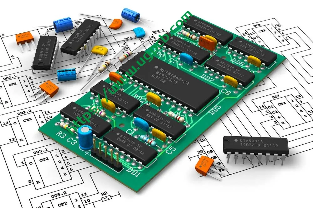
両面スルーホール PCB は 3 つのコア技術で動作します:
1. 両面配線 — FR-4絶縁基板の上面と下面の両方に導体回路パターンをエッチング, コンポーネントを両側に配置できるようにする. これにより、回路密度と設計の柔軟性が大幅に向上します。.
2. メッキスルーホール (PTH) 相互接続 — 穴あけ後, 無電解銅めっきと電解銅めっきにより穴壁に導電層を形成. これにより低抵抗が生まれます, 最上層と最下層間の信頼性の高い電気接続. IPC-6012Fクラスに準拠 2, 穴壁の最小平均メッキ銅厚は ≥ である必要があります。 20 μm.
3. 部品の組み立てとはんだ付け — コンポーネントは穴を通して取り付けられます (tht) または表面実装 (SMT) リフローまたはウェーブはんだ付けによる電気接続, 完全に機能する PCBA を製造する (印刷回路基板アセンブリ) モジュール.
V. 製品分類
リジッドプリント基板の IPC-6012F 分類システムによる, UGPCBの製品は次のように分類されます:
| 分類次元 | カテゴリ |
|---|---|
| 構造別 | メッキスルーホール付きリジッドプリント基板, 両面 (IPC-6012F型 2) |
| パフォーマンスクラス別 | クラス 2 (専用サービス用電子機器) |
| 基板材質別 | FR-4 エポキシガラスファブリックラミネート (IPC-4101/21) |
| レイヤーカウントごとに | 2-レイヤーボード |
| 表面仕上げによる | 鉛フリーHASL |
| 可燃性評価による | UL 94 V-0 |
アプリケーションドメイン別, この商品は以下に該当します 一般産業グレード両面PCB カテゴリ, 家庭用電化製品に適しています, 産業用制御, 通信機器, パワーアダプター, およびその他の中程度の信頼性のアプリケーション.
VI. 材料構成
6.1 基板 — FR-4 銅張積層板
FR-4 は、電子グレードのガラス織布を補強材として、エポキシ樹脂をバインダーとして構成されたガラス強化エポキシ積層板です。, 高温高圧下で固める. そのUL 94 V-0 可燃性評価とは、垂直燃焼試験における燃焼性を意味します。, 材料は内部で自己消火します 10 10秒間の炎を2回照射した後、それぞれ数秒後, 綿に引火する炎の滴りはありません.
6.2 銅箔 — 1/1 オズ
1オンス (1 オズ) 銅箔の厚さは 35 μm (1.37 ミル). UGPCB は使用します 1 両方の外層に OZ 銅 (指定された 1/1 オズ), 両側で等しい電流容量と導電率を確保.
6.3 表面仕上げ - 鉛フリー HASL
鉛フリー HASL では、PCB を溶融した鉛フリーはんだに浸漬します。 (通常はSn-Cu, Sn-Cu-Ni, またはSn-Ag-Cu合金), 次に、高圧熱風ナイフを使用して、余分なはんだを平らにして除去します。. これでユニフォームが出来上がります, 銅表面にはんだ付け可能な保護コーティング. このプロセスは IPC-6012F 要件および RoHS 環境指令に準拠しています。.
6.4 はんだマスクと凡例
-
緑色のはんだマスク — パッドを除くすべての回路領域をカバー, 断熱材を提供する, 酸化防止, 短絡防止.
-
白いシルクスクリーンの伝説 — コンポーネントの参照指定子を識別します, 極性マーカー, ボードの部品番号, アセンブリとデバッグを容易にするリビジョンレベル.
Ⅶ. 製品性能
7.1 電気性能
| パフォーマンスパラメータ | 価値 | 参照標準 |
|---|---|---|
| 誘電率 (DK) @ 1 GHz | 4.2-4.5 | IPC-4101 |
| 損失係数 (Df) @ 1 GHz | ≤ 0.020 | IPC-4101 |
| 絶縁抵抗 | ≧ 10^12 Ω | IPC-6012F |
| 耐電圧 | 耐電圧あたり | IPC-6012F |
7.2 機械的性能
| パフォーマンスパラメータ | 価値 | 参照標準 |
|---|---|---|
| 板厚 | 1.0 mm± 10% | IPC-6012F |
| 銅剥離強度 | ≥ 1.1 N/mm | IPC-6012F |
| 可燃性評価 | UL 94 V-0 | UL規格 |
| TG (ガラス転移温度) | 130–140℃ | IPC-4101 |
7.3 信頼性
IPC-6012Fクラスに準拠 2 要件, 製品は次の信頼性検証に合格する必要があります:
-
熱ストレステスト (288℃, 10 秒, 層間剥離や膨れがないこと)
-
メッキスルーホール銅密着性試験 (最小平均穴壁銅厚 ≥ 20 μm)
-
はんだ付け性試験
-
導通・絶縁抵抗試験
VIII. 製品構造
UGPCB の両面スルーホール PCB は対称 2 層構造を特徴としています. 上から下へ:
-
最上位の凡例レイヤー (白いシルクスクリーン)
-
上部ソルダーマスク層 (グリーンインク)
-
上部銅箔層 (1 オズ, 35 μm)
-
FR-4 絶縁基板 (1.0 mmの厚さ)
-
下部銅箔層 (1 オズ, 35 μm)
-
下部ソルダーマスク層 (グリーンインク)
-
最下部の凡例レイヤー (白いシルクスクリーン)
-
メッキスルーホール (PTH) — 銅メッキの穴壁により基板の厚さ全体に広がり、層間相互接続が可能になります
IX. 製品の特徴
-
高い配線密度 — 両面配線により、片面ボードよりも 60% ~ 80% 高い密度が実現します。, より複雑な回路設計をサポート.
-
信頼性の高いスルーホール相互接続 — メッキスルーホール (PTH) テクノロジーにより層間の長期的な電気的信頼性が保証されます, IPC-6012F クラスを満たす穴壁銅厚 2 要件 (≥ 20 μm平均).
-
優れた難燃性 — FR-4 基板は UL に適合 94 V-0 可燃性評価, 異常な動作条件下での安全性の確保.
-
鉛フリーで環境に優しい — 鉛フリーの HASL 表面仕上げは RoHS 環境指令に準拠しています.
-
ファインピッチ回路能力 — 最小線幅 0.32 mm、最小間隔は 0.37 mm 媒体に対応- 高密度回路設計まで.
-
優れた寸法安定性 — FR-4の低吸水性 (≤ 0.10%) 湿気の多い環境でも寸法変化を最小限に抑えます, 組み立て精度の維持.
-
成熟した製造プロセス - と 1.0 mmの板厚と 0.236 mm最小穴径, のみのアスペクト比 4.24:1 成熟したプロセスを可能にする, 高収量, 短いリードタイム.
x. 製造工程の流れ
UGPCBの標準両面スルーホールPCB製造プロセス:
1. 入荷検査 → FR-4銅張積層板の厚みを確認する, 銅箔の品質, および視覚的な欠陥.
2. 切断 → 大判銅張積層板を作業パネルサイズにカット (86.9 × 73.58 mm).
3. 掘削 → 高精度 CNC ボール盤を使用して、ガーバー ドリル ファイルに従ってすべてのスルーホールを穴あけします。 (最小直径 0.236 mm).
4. メッキスルーホール (PTH) → 無電解銅蒸着により穴壁に薄い銅シード層を蒸着します。.
5. パネルメッキ → 銅を電解メッキして、穴の壁と表面の銅を目標の厚さに堆積します (1 オズ).
6. パターン転写 → ドライフィルムをラミネートする, さらす, 現像して回路パターンレジストを形成します.
7. エッチング → 保護されていない銅をエッチングして除去し、最終的な回路パターンを形成します.
8. ストリッピング → 回路パターンからレジストのドライフィルムを除去します。.
9. ソルダーマスクの塗布 → 緑色のソルダーマスクインクを塗布, さらす, パッドを露出するように開発します.
10. 表面仕上げ → 鉛フリーHASL.
11. 凡例の印刷 → スクリーン印刷の白いシルクスクリーンの凡例.
12. ルーティング / Vカット → 最終基板外形への CNC ルーティング.
13. 電気テスト → オープン/ショートの完全性を検証するためのフライング プローブまたはフィクスチャ テスト.
14. 最終的な品質管理 (FQC) → 目視検査, 次元サンプリング, そして発送用の梱包.
XI. アプリケーションシナリオ
UGPCB 両面スルーホール FR-4 PCB ボード, バランスの取れたパフォーマンスと成熟したプロセスを備えた, で広く使用されています:
11.1 家電
-
パワーアダプターと充電器
-
家電制御盤
-
スマートホームデバイス
11.2 産業用制御
-
PLCプログラマブルロジックコントローラー
-
産業用パワーモジュール
-
計器類とメーター
11.3 通信機器
-
ルーターとスイッチ
-
通信モジュール
-
信号変換装置
11.4 カーエレクトロニクス
-
車載充電器
-
ボディコントロールモジュール (安全性が重要ではない)
-
インフォテインメントシステム
11.5 医療機器
-
患者モニター補助ボード
-
携帯型医療機器 (クラス 2 該当する)
XII. 製品の利点と選択ガイド
12.1 UGPCB 両面スルーホール PCB を選択する理由?
-
IPC準拠のプロセス制御 — 素材選びから製品の完成まで, IPC-6012Fに完全準拠, IPC-4101, およびその他の国際規格.
-
高精度の製造 — 最小穴径 0.236 mm、最小線幅は 0.32 mm ミートミディアム- 高密度設計要件に対応.
-
環境コンプライアンス — 鉛フリーの HASL 表面仕上げは RoHS に準拠しています 2.0 指令.
-
実証済みの信頼性 — FR-4 基板は数十年にわたって市場で検証されており、一貫した性能を備えています.
-
迅速な配達 — 標準仕様は原材料を豊富に取り揃えています, 確実なリードタイムの確保.
12.2 選定基準
UGPCB 両面スルーホール PCB は、プロジェクトがこれらの基準を満たしている場合に理想的な選択肢です。:
-
適度な回路の複雑さ 2 レイヤーは収容可能
-
動作周波数以下 1 GHz (FR-4 はこの範囲で優れたパフォーマンスを発揮します)
-
120℃以下の長期使用環境
-
高い価値を要求するコスト重視のアプリケーション
XIII. 見積もりを依頼する
UGPCB は、高品質の PCB 製造とターンキー PCBA サービスを世界中の顧客に提供することに尽力しています。. 標準仕様の両面スルーホール PCB が必要か、それともカスタム要件が必要か (特殊な板厚, 銅の重量, 表面仕上げ, インピーダンス制御, 等), UGPCB の専門家チームがエンジニアリング設計から量産まで完全にサポートします.
今すぐ見積もりを入手:
-
ガーバーファイルを送信する + 仕様 — 以内に見積もりを受け取ります 24 時間
-
試作から量産までサポート
-
製造のための自由な設計 (DFM) レビュー
連絡先:
📧販売に関するお問い合わせ: [sales@ugpcb.com]
🌐 ウェブサイト: [www.ugpcb.com]
XIV. データソース宣言
この文書で引用されている規格とデータは、次の権威ある組織から提供されています。:
-
IPC (エレクトロニクス産業をつなぐ協会): IPC-6012F リジッドプリント基板の認定および性能仕様 (9月 2023); IPC-4101 リジッド・多層プリント基板用基材仕様; IPC-2221 プリント基板設計に関する一般規格; IPC-7351 表面実装設計およびランドパターン規格の一般要件
-
UL (引き受けの研究所): UL 94 機器・家電部品のプラスチック材料の燃焼性試験に関する規格
-
ありません (全国電気製造者協会): FR-4 材料グレードの定義
-
業界標準の技術データ: FR-4の誘電率, 散逸係数, およびその他の材料特性パラメータ













