
eMMC PCB Package Substrate Product Overview
In today’s data-centric world, the performance and reliability of embedded storage are critical. EMMC (embedded MultiMediaCard) serves as the core storage unit in smartphones, 錠剤, IoT devices, and other consumer electronics. UGPCB, leveraging deep expertise in 高密度相互接続 (HDI) プリント基板の製造, offers specialized eMMC Package Substrate PCBs. Designed with HL832NS material in a 4-layer, ultra-thin configuration, this substrate is the essential platform for high-speed, stable electrical interconnection between the memory controller, NAND flash dies, そしてメインボード. It is the optimal solution for developing next-generation compact, high-capacity storage modules.
What is an eMMC Package Substrate PCB?
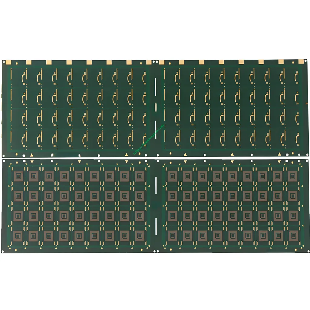
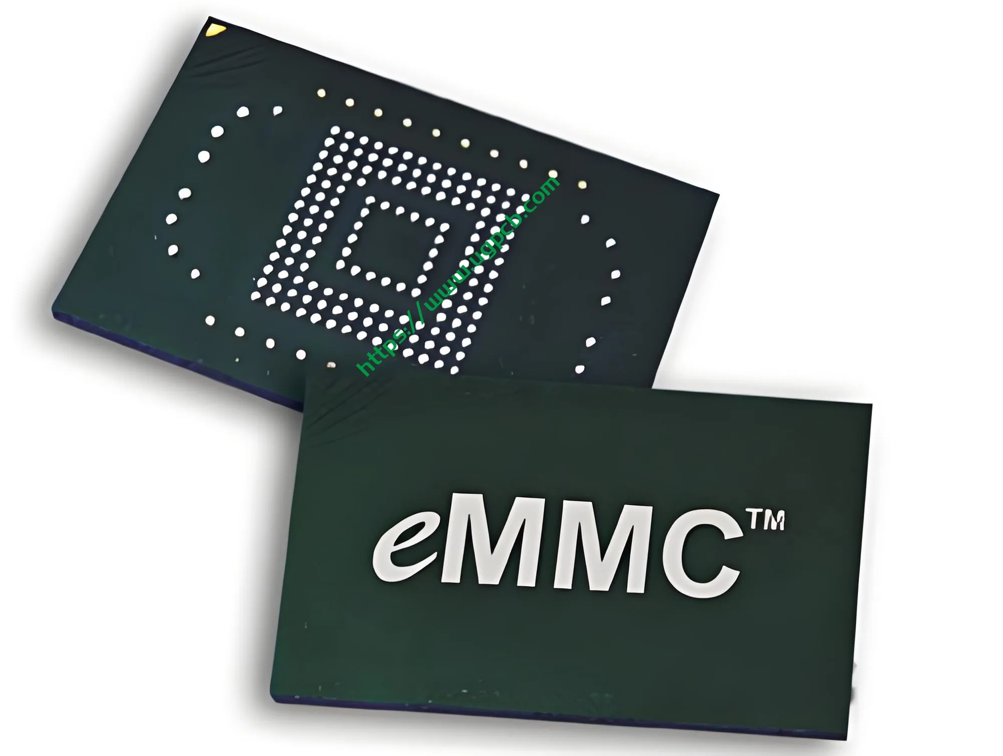
An eMMC Package Substrate PCB 特別なものです, miniaturized プリント基板 used internally within an eMMC chip package. It serves as the core interposer, providing the electrical connections and physical support between the storage controller silicon die, the NAND flash memory dies, and the external Ball Grid Array (BGA) インタフェース. Its design and manufacturing quality directly determine the signal integrity, 熱性能, and overall reliability of the final eMMC module.
デザインのハイライト & 主要な技術仕様
To meet the stringent demands of eMMC chips for high bandwidth and miniaturization, UGPCB’s eMMC substrate focuses on these critical design parameters:
-
High-Density Routing: Supports ultra-fine circuitry with minimum line width/space of 20µm.
-
Micro-Via Capability: 特徴 minimum via diameter of 0.1mm for high-density I/O fanout.
-
Stable Lamination: 4-layer construction with a controlled total thickness of 0.21mm, balancing electrical performance and mechanical strength.
-
High-Reliability Surface Finish: ソフトゴールド (同意する) plating provides an oxidation-resistant, low-resistance surface for reliable wire bonding or flip-chip attachment.
-
Precise Solder Mask: PSR-4000 AUS308 solder mask offers excellent insulation and chemical resistance.
それがどのように機能するか & 構造的特徴
それがどのように機能するか: The substrate acts as the internal “神経系” そして “power grid” of the eMMC module. Its conductive traces and micro-vias route command signals from the controller to the NAND flash dies and return data. Dedicated power and ground planes ensure stable, low-noise power delivery.
構造的特徴:
-
超薄型 & コンパクト: 0.21mm final thickness そして 11.5mm x 13mm unit size minimize space consumption.
-
Advanced Core Material: 上に構築 HL832NS, a high-performance laminate known for excellent thermal stability and low signal loss (低dk/df), crucial for heat dissipation.
-
Multi-Layer Architecture: The 4-レイヤースタックアップ (typically signal, 力, 地面) optimizes signal paths, reduces crosstalk, and controls impedance.
-
BGA Pad Array: The bottom side features a precise BGA pad layout for reliable surface-mount technology (SMT) assembly of the entire module onto the host motherboard.
Primary Application & ユースケース
Primary Application: Core interconnection platform within EMMC 5.1 and above チップパッケージ.
典型的なアプリケーション (ユースケース):
-
スマートフォン & タブレット: Primary internal storage.
-
Smart TVs & Set-Top Boxes: System storage and caching.
-
IoTデバイス: スマートウォッチ, smart home hubs requiring compact embedded storage.
-
産業用制御システム: Embedded devices demanding high data reliability.
-
Automotive Infotainment: Storage modules meeting automotive-grade stability requirements.

分類 & 材料構成
-
分類: Can be categorized by application grade: 消費者, 産業用, and Automotive (this model is tailored for consumer & high-end industrial applications).
-
Material Stack-Up:
-
Core Laminate: HL832NS 高Tg, Low-Loss material.
-
Conductive Layers: High-purity electrolytic copper foil.
-
はんだマスク: PSR-4000 AUS308 (緑, matte/gloss optional).
-
表面仕上げ: エレクトロレスニッケルイマージョンゴールド (同意する – ソフトゴールド).
-
Performance Advantages & 主な特長
-
優れた信号の完全性: Controlled impedance and low-loss HL832NS material ensure stable high-speed data transfer.
-
高い信頼性: Stringent process controls and material selection guarantee long-term durability.
-
Effective Thermal Management: The laminate’s good thermal conductivity aids in heat dissipation from the active dies.
-
Tight Manufacturing Tolerances: 20µm line/space and 0.1mm micro-vias demonstrate 高度な HDI PCB 製造業 専門知識.
-
End-to-End Solution: UGPCB provides collaborative support from substrate design review そして PCB製造 に ラピッドPCBAプロトタイピング.
製造工程の概要
Our eMMC Package Substrate manufacturing follows a stringent HDI PCB process flow:
Material Prep → Inner Layer Imaging → Lamination → Laser Drilling (0.1mm vias) → Via Metallization → Outer Layer Imaging (20µm lines) → ソルダーマスク塗布 (PSR-4000) → Surface Finishing (ソフトゴールド) → Electrical Testing → Routing/Scoring → Final Inspection & 包装.
Why Choose UGPCB for Your eMMC Package Substrate?
Choosing UGPCB means partnering with an expert in memory chip substrate manufacturing. We understand the technical evolution of storage interfaces and offer full-chain support to ensure your product excels in performance, 料金, と信頼性.
Contact us today to discuss your eMMC Package Substrate requirements and request a quotation. Let UGPCB’s precision engineering be the reliable foundation for your next-generation storage solutions.


