
UGPCB 標準 2 層リジッド PCB: 要求の厳しいアプリケーション向けの信頼性の高い 1.6mm FR-4 回路基板
現代のエレクトロニクスの中心, の プリント基板 (プリント基板) 基礎的なプラットフォームとして機能します, コンポーネントを相互接続し、信号を正確にルーティングします。. UGPCB 標準 2 層リジッド PCB, 堅牢な構造で作られています 1.60mmの厚さ そして高性能 FR-4 TG150材, 耐久性の最適なバランスを実現, 電気性能, 幅広い用途に適した費用対効果. これ 両面PCB プロトタイプおよび中程度の複雑さの電子デバイス向けの実証済みのソリューションです.
製品の定義 & 分類
技術分類:
-
レイヤーカウントごとに: 両面PCB / 2層PCB
-
基板剛性別: リジッドPCB
-
ベース素材によって: ガラスエポキシ (FR-4) プリント基板
-
可燃性評価による: UL94V-0 (FR-4固有の)
-
アセンブリの互換性による: スルーホールテクノロジー (tht) および表面実装技術 (SMT) 対応PCB.
この商品は、 両面回路基板 絶縁 FR-4 コアの両側に銅張積層板で構築. 層間の電気接続はメッキスルーホールを介して実現されます。 (PTH). The 1.60mm (約 1/16 インチ) ボードの厚さ 業界標準です, 優れた機械的安定性を提供します.
工事 & 材料仕様
レイヤースタックアップ:
これ 2 層リジッドPCB 構造は次のとおりです (上から下へ):
-
上部ソルダーマスク (白): はんだブリッジを防止する絶縁層.
-
上部銅層 (1 オンス, ~35μm): エッチングして導電性トレースとパッドを形成.
-
絶縁コア基板 (FR-4, Tg150): 機械的サポートと電気絶縁を提供します.
-
下部銅層 (1 オンス, ~35μm): エッチングして最下層回路を形成.
-
底部はんだマスク (白): 絶縁保護層.
-
シルクスクリーンの伝説 (黒): コンポーネント指定子, ロゴ, とマーキング.
主要な資料:
-
ベースラミネート: FR-4 TG150. これは、ガラス転移温度を備えた難燃性ガラス強化エポキシ積層板を示します。 (TG) 150℃以上. 優れた機械的強度を提供します, 電気断熱, 熱信頼性と リジッドプリント基板, 業界で最もコスト効率の高い選択肢となります.
-
銅箔: 標準1オンス (オンス) 最適な導電性と電流容量を実現する電着銅.
-
表面仕上げ: 鉛フリー熱風はんだレベリング (出血). コスト効率が高く信頼性の高い プリント基板表面仕上げ 優れたはんだ付け性を実現, 良好な保存期間, 酸化に対する堅牢な保護.
-
インク: 高品質の写真イメージング可能な白色ソルダーマスクインクと耐久性のある黒色エポキシシルクスクリーンインク.
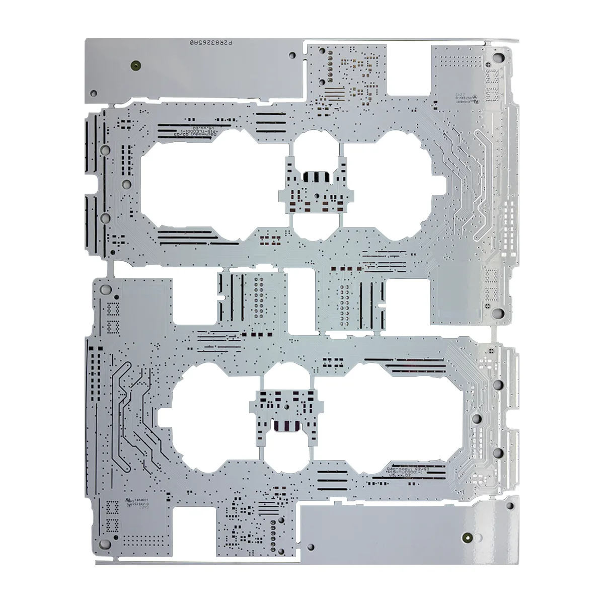
(画像の提案: PCB積層構造の断面図)
すべてがかかる: の詳細断面図 2 銅を示す層のリジッド PCB, FR-4コア, およびソルダーマスク層.
設計ガイドライン & 動作原理
設計上の重要な考慮事項:
-
ビアデザイン: 配線スペースを最大化します。 両面 プリント基板設計 メッキスルーホールを戦略的に配置することにより (pths) 層間接続用.
-
トレース幅/間隔: 1オンスの銅の場合, 標準の最小トレース/スペースは 6mil/6mil です (~0.15mm) 信頼性の高い製造性と電流容量を確保するため.
-
パッド & 穴付きアニュラーリング: 強力な接続を保証するために、ドリル穴に対して適切なパッド サイズを確保してください。 PCBアセンブリ と信頼性.
-
はんだマスク & シルクスクリーン: 白いソルダーマスクは、作業中の目視検査に役立ちます。 SMTアセンブリ, 一方、透明な黒いシルクスクリーンは、 PCBプロトタイピング そして修理する.
動作原理:
PCB は機能を生成しませんが、事前に定義された導電経路を通じて機能を有効にします。. エッチングされた銅トレースがディスクリート配線を置き換えます, コンポーネント間の電気接続を提供する. 絶縁FR-4基板により短絡を防止. メッキスルーホール (pths) 垂直導管として機能する, 上と下を繋ぐ PCB 銅層, これにより、片面基板と比較して利用可能な配線領域が 2 倍になり、設計の柔軟性が向上します。.
性能特性 & 利点
-
高い信頼性: The FR-4 TG150基板 Tg未満の環境でも安定した性能を保証します, 優れた熱的および機械的安定性を提供します。 リジッド回路基板.
-
優れた電気特性: 低い誘電率と誘電正接により、ほとんどのデジタルおよびアナログ回路の信号整合性要件をサポートします。.
-
高い製造性: The 1.6mm 標準PCB 厚さ そして 鉛フリーHASL プロセスが成熟している, 高収量の確保, コスト管理, リードタイムが速い.
-
優れたはんだ付け性: HASL仕上げによりフラットな仕上がりになります。, 湿潤性のある表面は両方に最適です スルーホールはんだ付け そして SMTはんだ付けプロセス.
-
明確な識別: 黒い凡例が付いた高コントラストの白いはんだマスクにより、効率的な作業が容易になります。 プリント基板 検査, テスト, そしてやり直し.
-
環境コンプライアンス: 鉛フリー HASL 仕上げは RoHS およびその他の環境指令に準拠しています.
標準的な製造工程の流れ
UGPCB は、当社全体を通じて IPC 標準に準拠しています。 PCB製造プロセス:
パネル化 → 穴あけ → 無電解銅めっき → ドライフィルムラミネート & イメージング → 銅メッキ → エッチング → ソルダーマスク塗布 & 硬化→シルク印刷→表面仕上げ (鉛フリーHASL) → プロファイリング/ルーティング → 電気テスト (飛行プローブ) → 最終自動光学検査 (あおい) → 包装 & 出荷.
主要なアプリケーション & ユースケース
この多彩な 2層リジッドPCB 信頼性と価値のバランスが求められる業界で広く使用されています:
-
産業用制御: PLCインターフェース, センサーモジュール, モータードライブ, HMIコントローラボード.
-
家電: スマート アプライアンス コントローラー, オーディオアンプ, 電源, 教育キット.
-
通信: ルーター/スイッチ周辺ボード, RFアンテナモジュール, ネットワーク監視ユニット.
-
カーエレクトロニクス: インフォテインメントシステム, 照明制御モジュール, ボディコントロールモジュール (安全性が重要ではない).
-
パワーエレクトロニクス: スマートメーター基板, UPS制御ボード, ソーラーインバータ回路.
-
テスト & 測定: データ収集カード, 計器制御パネル, ハンドヘルドテスターボード.
2 層 PCB のニーズに UGPCB を選択する理由?
UGPCB を選択するということは、信頼できるパートナーと提携することを意味します。 PCBメーカー 品質へのこだわり. 私たちは以下を専門としています PCBプロトタイプ 中量生産, すべての基板に厳格な電気試験と IPC-A-600 ベースの検査を実施. シンプルなものから 2 レイヤーボード 複雑な多層設計まで, 専門家を提供します 製造用の PCB 設計 (DFM) サポートと合理化されたサプライチェーン.
1.6mm FR-4 2 層 PCB プロジェクトの競争力のある見積もりと迅速なリードタイムについては、今すぐお問い合わせください。!
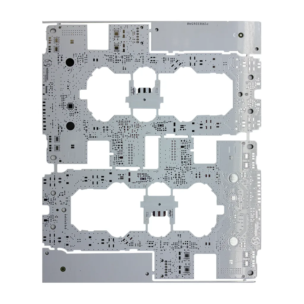
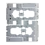
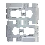
(画像の提案: さまざまなデザインの完成した PCB のギャラリー)
すべてがかかる: いろいろなギャラリー 2 UGPCB 製の白色ソルダーマスクを使用した層状リジッド PCB の例.


