
High-Performance 12-Layer ENIG + Gold Finger PCB 製品の概要
The 12-Layer Gold Finger PCB is a hallmark product in the high-end プリント基板 業界, engineered specifically for electronic equipment demanding extreme reliability, stable electrical connections, and frequent plugging/unplugging cycles. UGPCB employs advanced manufacturing processes and premium materials (FR-4 TG170), combining 2m” エレクトロレスニッケルイマージョンゴールド (同意する) surface finish with 30m” Hard Gold Finger Plating テクノロジー. We deliver a comprehensive high-reliability PCB solution for applications ranging from industrial controls to advanced communication systems.

製品の定義
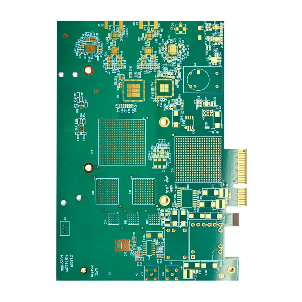
A Gold Finger PCB refers to a circuit board featuring a series of exposed, rectangular contact pads plated with thick gold (“fingers”) along one edge. These boards are designed for direct insertion into a matching connector slot, establishing a stable, pluggable connection for electrical signals and power between devices. この商品は、 12-多層PCB with a standard thickness of 1.60mm, offering an optimal balance between complex circuit integration and mechanical robustness.
設計上の重要な考慮事項
-
Gold Finger Area Design:
-
Chamfer (Bevel) Edge (Typically 20-45°): Facilitates smooth insertion into the connector—a critical aspect of ゴールドフィンガー プリント基板設計.
-
Lead-in (Trace Fanout): Connections from the gold fingers to internal traces must have smooth curves, avoiding right angles to prevent stress concentration and plating cracks.
-
Solder Mask Clearance (Solder Mask Define): The gold finger area requires precise solder mask opening to ensure a clean, exposed plating surface.
-
-
インピーダンス制御 & 信号の完全性: として 12-layer precision PCB, strict impedance control (例えば。, 50Ω シングルエンド, 100Ω差動) for high-speed signal layers is essential. Stack-up design must be optimized via simulation to minimize crosstalk.
-
熱 & Reliability Management: High-Tg material, coupled with a well-designed via structure, ensures the 多層PCB operates stably in elevated temperature environments. メッキスルーホール (pths) should be avoided at the root of gold fingers to prevent fluid entrapment and structural weakness.
それがどのように機能するか & 構造
This PCB facilitates complex circuit interconnections through its internal 12 導電層. The core functionality resides in the Hard Gold Plated Fingers. The durable 30-microinch gold plating provides excellent conductivity, 耐酸化性, そして耐摩耗性. When the board is inserted into a backplane or card-edge connector, the gold fingers make tight, low-resistance electrical contact with the connector’s spring contacts, transmitting signals and power. The board core uses FR-4 TG170, providing solid mechanical support and electrical insulation.
コア材料 & 仕様
-
基本材料: FR-4 TG170. A high-performance epoxy glass laminate.
-
高いガラス転移温度 (Tg ≥ 170°C): Significantly enhances the PCB’s mechanical stability and heat resistance under high-temperature operating conditions, preventing delamination and Z-axis expansion.
-
優れた電気特性: 低誘電率 (DK) および散逸率 (Df), suitable for mid-to-high frequency applications.
-
高い機械的強度: Ensures the 1.6mm thick PCB board resists bending and warping in mating/unmating and high-vibration environments.
-
-
表面仕上げ:
-
Board Surface: エレクトロレスニッケルイマージョンゴールド (同意する, 2m”): アパートを提供します, coplanar surface for reliable soldering of fine-pitch components and offers excellent oxidation resistance.
-
ゴールドフィンガーズ: Selective Electroplated Hard Gold (30m”): High hardness, superior abrasion resistance, and extended mating cycle life, capable of withstanding 500+ insertion/withdrawal cycles with ease.
-
主な特長 & 利点
-
Unmatched Reliability: FR-4 TG170 high-Tg material そして 12-layer precision lamination ensure long-term stability in harsh operating conditions.
-
Extended Mating Cycle Life: 30m” thick hard gold fingers far exceed standard plating thickness, offering exceptional wear resistance—the ideal choice for high-durability plug-in PCBs.
-
優れた信号の完全性: The multilayer design provides uninterrupted reference planes for high-speed signals, and controlled impedance guarantees signal quality.
-
Robust Thermal & 機械的性能: The 1.60mm standard thickness combined with high-Tg material delivers superior rigidity, 熱管理, and dimensional stability.
-
Comprehensive High-End Solution: から 多層 PCB製造 に specialty surface finishing (同意する + Selective Gold), UGPCB provides full-process control, ensuring consistent, 高品質の結果.
製造工程の流れ
Panelization → Inner Layer Imaging → Lamination (12-層) → Drilling → Desmear & Electroless Copper Deposition → Outer Layer Imaging → パターンメッキ (for Hard Gold Fingers) → Etching → Solder Mask Application → ENIG Surface Finish → Gold Finger Beveling → Electrical Test (飛行プローブ / Fixture) → 最終自動光学検査 (あおい) → 包装.
主要なアプリケーション & ユースケース
This product is the core component of high-end electronic devices requiring direct board-to-board plug connections または integration into backplane systems.
-
産業用制御システム: PLCモジュール, industrial computer motherboards, サーボドライブ, I/O interface cards.
-
通信 & Networking Equipment: Router/switch line cards, optical transceiver modules, baseband processing units.
-
医療エレクトロニクス: Data acquisition and processing boards for advanced medical imaging systems (例えば。, CT scanners, ultrasound machines).
-
テスト & 測定器: Plug-in modules for high-end oscilloscopes, スペクトラムアナライザ, and Automated Test Equipment (食べた).
-
航空宇宙 & 防衛電子機器: Mission-critical avionics systems and radar signal processing modules where reliability is paramount.

科学製品の分類
-
レイヤーカウントごとに: 多層レイヤー数 / Multilayer Circuit Board (≥8 layers, 具体的には 12 レイヤー).
-
By Special Feature/Process: ゴールドフィンガー (Gold Edge Connector) プリント基板, Mixed Surface Finish PCB (同意する + Selective Hard Gold).
-
By Material Property: 高Tg (TG170) プリント基板, FR-4 Series PCB.
-
アプリケーショングレード別: Industrial-Grade PCB, Telecom-Grade PCB, High-Reliability PCB.
Why Choose UGPCB’s 12-Layer Gold Finger PCB?
We understand that a reliable Gold Finger PCB is the foundation of your high-end equipment’s stable operation. 深い専門知識を活用して、 多層 プリント基板の製造 そして specialty surface finish processes, UGPCB guarantees that every board delivered meets military-grade reliability standards with commercial-grade delivery efficiency. 私たちが提供するのは製品だけではありません, but a customized PCB solution.
今すぐ当社の技術営業チームにお問い合わせください to discuss your project requirements, receive a detailed quote, and qualify for a free design-for-manufacturability (DFM) レビュー and sample program. Partner with UGPCB for your most demanding 12 層回路基板 アプリケーション.


