
最先端のチップの中心には基板があります, 爪ほどの大きさしかありませんが、何万もの複雑な回路が交差しています, システム全体のパフォーマンスと安定性を静かに決定します。.
The ICパッケージ基板 半導体チップパッケージングにおけるコアキャリアです. 電気信号接続の確立を担当します, 電力供給, 物理的なサポート, 熱放散, 半導体ダイと外部間の保護 プリント基板 (プリント基板). そのパフォーマンスはチップのシグナルインテグリティを直接決定します, 熱効率, そして最終製品の信頼性.
LGAを活用したIC基板 (ランドグリッドアレイ) 梱包, 底面にフラットアレイパッドのユニークなデザインを採用, 高性能を実現するための重要な選択肢になりつつあります, 高密度チップパッケージング.
01 製品の概要: 意味 & コア仕様
ICパッケージ基板, ICキャリアとも呼ばれる, チップパッケージングプロセスにおいて最も価値の高い主要材料です. 半導体ダイの微視的な世界と PCB 回路の巨視的な世界の間のトランスレーターとして機能し、橋渡しをします。.
簡単に言えば, 内部の精密マイクロ回路を通じて, 高密度に充填された電極パッドを変形させて拡張します。 (ミクロンスケールで) はんだ付けやメイン PCB への接続に適したスケールでダイ上に配置.
LGA IC基板 UGPCB は、高密度向けに特別に設計されたハイエンドの相互接続キャリアです。, 高性能チップ. 基本モデルのコア仕様により、その機能の境界が定義されます。.
以下の表は、製品の主要な物理的および電気的パラメータの概要を明確に示しています。:
| パラメータのカテゴリ | 仕様 | 意義 & 含意 |
|---|---|---|
| 基礎工事 | 材料: SI165 / レイヤー: 4 / 厚さ: 0.4mm | 薄型高機能ラミネートを採用, 多層相互接続, コンパクトなスペース要件を満たす. |
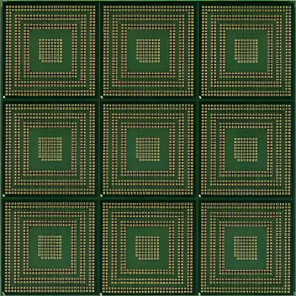
| 外形寸法 | ユニットサイズ: 8mm×8mm | チップスケールパッケージに最適 (CSP) または小型化されたパッケージ, 全体的なデバイススペースを節約する. |
| 線の精度 | 分. 線幅: 40μm / 分. 行間: 100μm | 高密度相互接続を表します (HDI) 能力, 限られたエリア内でより多くの信号ルートを可能にする. |
| Microviaテクノロジー | 分. ドリルサイズ: 0.1mm (100μm) | 高密度の層間伝導が可能, 複雑な多層相互接続の基礎. |
| 表面仕上げ | はんだマスク: PSR-2000 BL500 / 表面処理: エネピック | はんだ付けの信頼性を確保. エネピグは優れた, 長持ちするはんだ付け可能な表面. |
LGA パッケージングの特徴は、平らな金属パッドの配置です。 (土地) 基板底部の完全または部分的なアレイで, BGA のはんだボールとは対照的に (ボールグリッドアレイ).
この設計により、PCB にはんだ付け時の共平面性制御が向上し、電気経路が短くなります。, 高周波・高速信号伝送に有利.
02 技術的な詳細: 構造, デザイン & 動作原理
LGA IC 基板は複雑なマイクロシステム エンジニアリングの成果です. そのコア構造は通常、次のとおりです。, 上から下まで: ダイアタッチエリア (フリップチップまたはワイヤボンド接続用), マルチレイヤ HDI ルーティング レイヤ, 組み込み受動部品 (オプション), 底面のLGAパッドアレイ.
デザインの焦点 極小エリア内で効率的かつ信頼性の高い電気相互接続を実現することに重点を置いています。. 40μmの最小線幅と100μmの間隔がコアデザインルールです, 電流容量の正確な計算が必要, インピーダンス制御, および信号クロストーク.
組み込み技術 最先端のデザイン方向性です. 抵抗やコンデンサなどの受動部品の埋め込みが含まれます。, あるいはICダイさえも, 基板層内に直接. これにより回路経路が大幅に短縮されます, 電気的性能を向上させる, 信頼性を高める, 表面スペースを節約します.
動作原理 高速道路の信号と電力のインターチェンジに例えることができます. チップによって生成された信号は、マイクロバンプまたは金ワイヤを介して基板の最上層に入力されます。. その後、それらは再分配され、基板の複雑な経路を通ってルーティングされます。, 底部の LGA パッドを介してマザーボード PCB に安定かつ効率的に送信される前の多層回路.
このプロセス全体を通して, 基板自体の低誘電損失, 安定したインピーダンス, 信号の歪みを防ぐには、優れた熱性能が重要です。, 電力減衰, チップの過熱.
03 物質科学: The “肉 & 血” 基板の
基板の性能の源泉はその構成材料にあります. 当社の基板のコア材料は SI165, 高性能有機樹脂系積層体. IC基板領域では, ラミネートは最大のコスト要素です, 通常、以上を占めます 30% 総費用のうち. その特性が基板の電気的特性を決定します。, サーマル, そして機械的性能.
現在主流のハイエンド有機ラミネートには次のものがあります。:
-
BT (ビスマレイミド トリアジン) 樹脂: 持ちこたえる 70% 世界市場シェア. 高い耐熱性で知られています, 高弾性率, 熱膨張係数が低い (CTE), メモリチップのパッケージングに広く使用されています.
-
ABF (味の素ビルドアップフィルム): 主に日本の味の素社から供給されています. ハイエンドのロジックチップに推奨 (CPU, GPU) 絶縁性に優れ、極細線パターニングに適しているため.
コアラミネートを超えて, 銅箔が導電性トレースを形成します, ラミネートには特殊なプリプレグが使用されます, 一方 PSR-2000 BL500 ソルダーマスク そして エネピグ表面仕上げ 最終的な保護およびはんだ付け可能なバリアを形成します.
高精度LGA基板はチップの小型化と性能向上の基礎となる, 標準的な PCB をはるかに超える内部配線密度.
04 ものづくりの芸術性: 原材料から精密部品までの道のり
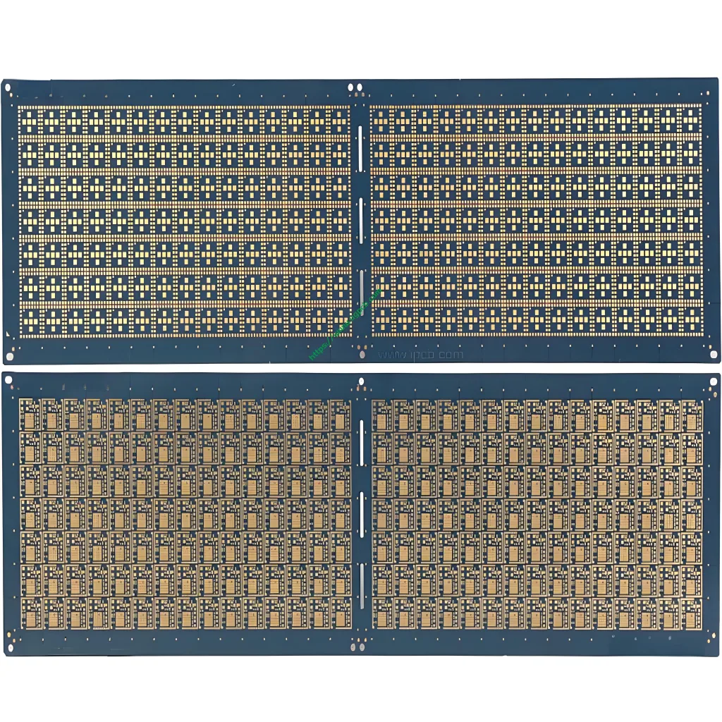
IC 基板の製造は、最も複雑で精度が要求される分野です。 PCB製造. そのコアプロセスフローは標準と類似点を共有していますが、 多層PCBの製造, 精度管理が大幅に厳しくなりました.
主要なプロセスには内層イメージングが含まれます, ラミネーション, レーザー/機械掘削, ホールメタライゼーション, 外層イメージング, 表面仕上げ, はんだマスクの塗布, および配線/電気テスト.
40μmレベルの線幅を実現, 製造業では主に 修正セミアディティブプロセス (msap). このプロセスには、ラミネート上に化学銅の薄い層を堆積することが含まれます。, 電気めっきにより、目的の回路パターンを構築します。, 最後に余分な薄い銅をエッチングで除去します。. これにより、従来の減算法よりも細い線が可能になります。.
穴あけ技術 も重要です. 100μmレベルのマイクロビア用, 機械による穴あけは限界に達している, 高精度のものを作る レーザー穴あけ 不可欠. より小さいものを作成できます, より正確なブラインドビアと埋め込みビア.
エネピグ表面仕上げ 最後の重要なステップです. ニッケルを順次堆積, パラジウム, とゴールド, LGA パッドに最高レベルのはんだ付け性能と信頼性性能を提供.
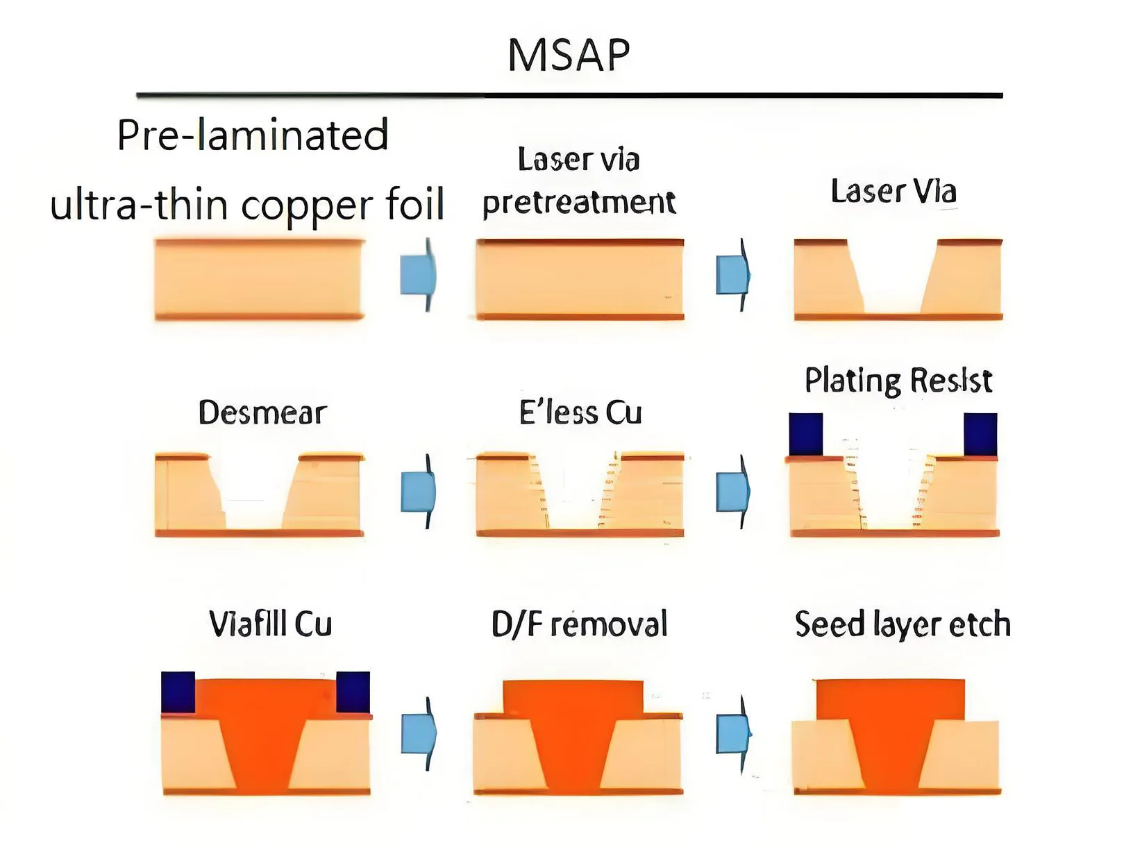
オルタナティブ: 修正されたセミアディティブ プロセスのステップを示す簡略図 (msap) 超微細な回路ラインの作成に.
05 アプリケーションの範囲: 多様な産業に電力を供給
LGA IC基板は単一製品ではありません. コアコンポーネントとして, ほぼすべての高度な電子システムの中心部に統合されています.
アプリケーションの状況は、提供するチップの種類と最終用途のアプリケーションに基づいて明確にマッピングできます。:
-
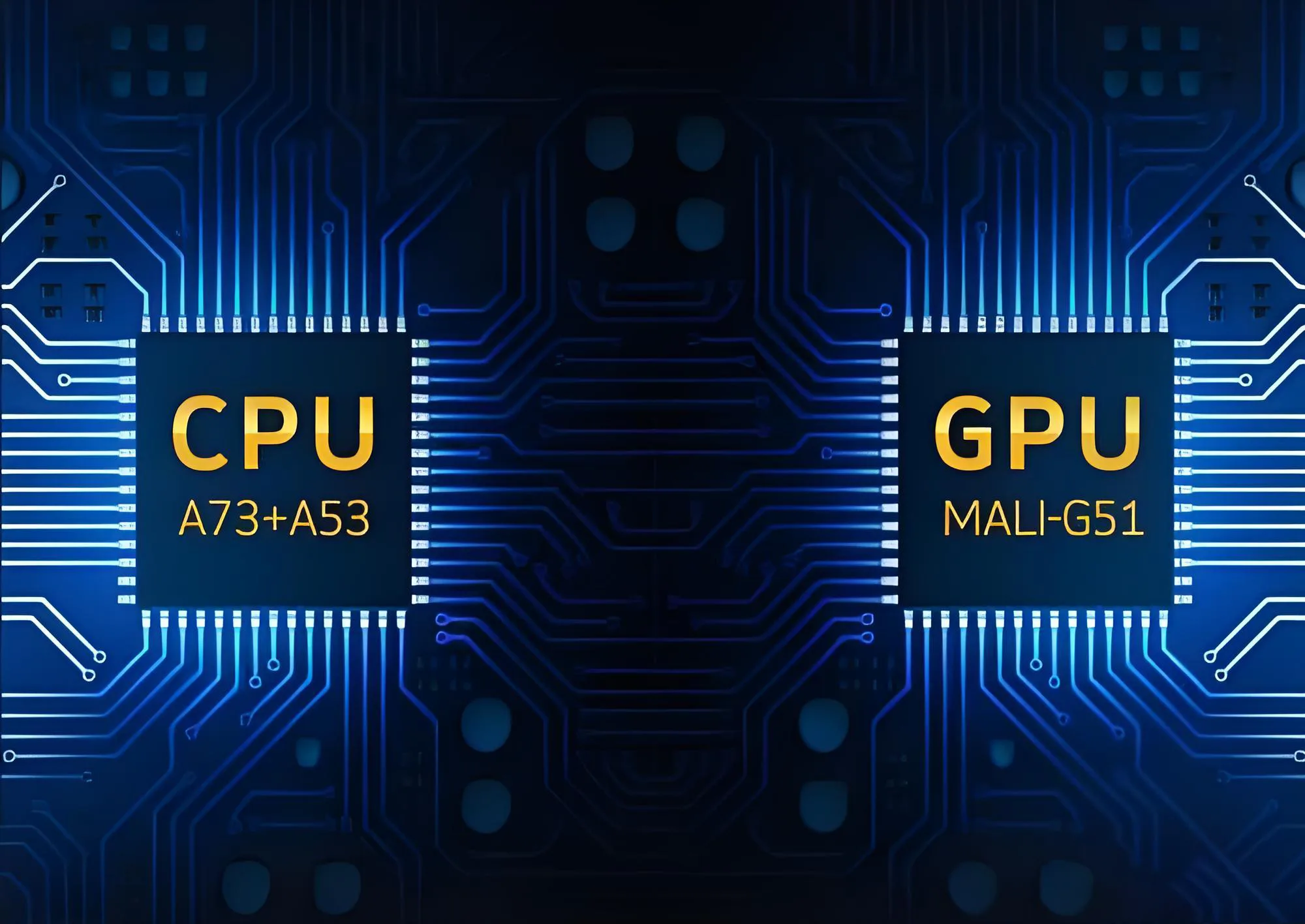
高性能コンピューティング (HPC): CPU, GPU, FPGA. この分野は基板に最も多くの要求を持っています, ABF マテリアルが必要です, 非常に高い配線密度, 優れた高速性能. これらの大型チップでは LGA パッケージングが普及しています.
-
メモリチップ: ドラム, NANDフラッシュ. 通常は成熟した BT 材料基板を使用します. 膨大な需要により基板市場の主力となっている.
-
コミュニケーション & RF: 5G/6G RFモジュール, パワーアンプ. 低損失の基板が必要, 高周波特性.
-
センサー & MEMS: 画像センサー, 慣性計測ユニット, マイク. 基板は特定のパッケージング形式と信頼性要件を満たさなければなりません.
-
カーエレクトロニクス & ai: 自動運転チップ, AIアクセラレータ. 自動車グレードの高い信頼性と堅牢なデータ処理機能を備えた基板を必要とする新たな成長分野.
世界のIC基板市場は、 $16.19 10億 2025, これらの下流アプリケーションの活発な成長によって推進されています.
06 今後の展望: テクノロジーの進化 & 業界の洞察
基板業界は、次のような状況と歩調を合わせて進化しています。, そしてドライブさえも, 半導体パッケージング技術の進歩. 現在 2 つの大きなトレンドが顕著です: 高密度の統合 そして 高度なパッケージングの融合.
ムーアの法則が物理的限界に近づくにつれて, 高度なパッケージングによるシステムパフォーマンスの向上が主要な経路となっている. のようなテクノロジーの台頭 システムインパッケージ (SiP) そして 2.5D/3D パッケージング 基板に前例のない要求を課す.
例えば, として使用される基板 インターポーザー 2.5D パッケージでは非常に高密度の TSV が必要です (スルーシリコン経由) 相互接続. 3Dスタッキングでは, 基板は、マルチダイの積層による重大な熱的および機械的ストレスの課題に耐える必要があります.
急成長 チップレット テクノロジーは基板をシステム統合ハブにさらに高めます. さまざまな機能とプロセスノードのチップレットには、基板を介した異種統合が必要, 設計の複雑さに対する究極のテストを提示する, ルーティング機能, および信号の完全性.
競争環境について, 世界のIC基板産業は寡占状態にある, 上位 10 社の合計市場シェアは、 80%. ハイエンド市場は日本の数社が独占している, 韓国, そして台湾. 中国本土企業は追いつくために努力している, ミッドエンドからハイエンド市場への躍進を加速, 国家政策の支援と市場の需要の両方によって促進される.
UGPCB の LGA IC 基板ソリューションは、この技術変革の最前線にあります. 8x8mm 基板には微細な回路だけが搭載されるわけではない, しかし、次世代の高性能コンピューティングへの巨視的な架け橋として機能します。.
世界的なデジタル化とインテリジェント化が進む中, クラウド データセンターからハンドヘルド スマート デバイスに至るまで、チップのパフォーマンスに対する飽くなき要求が続いています.


