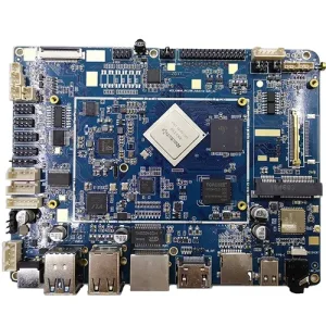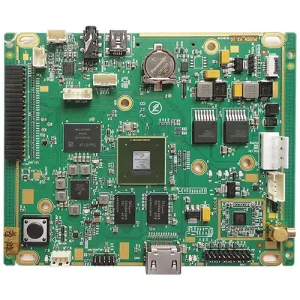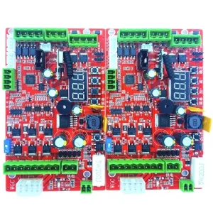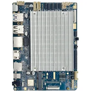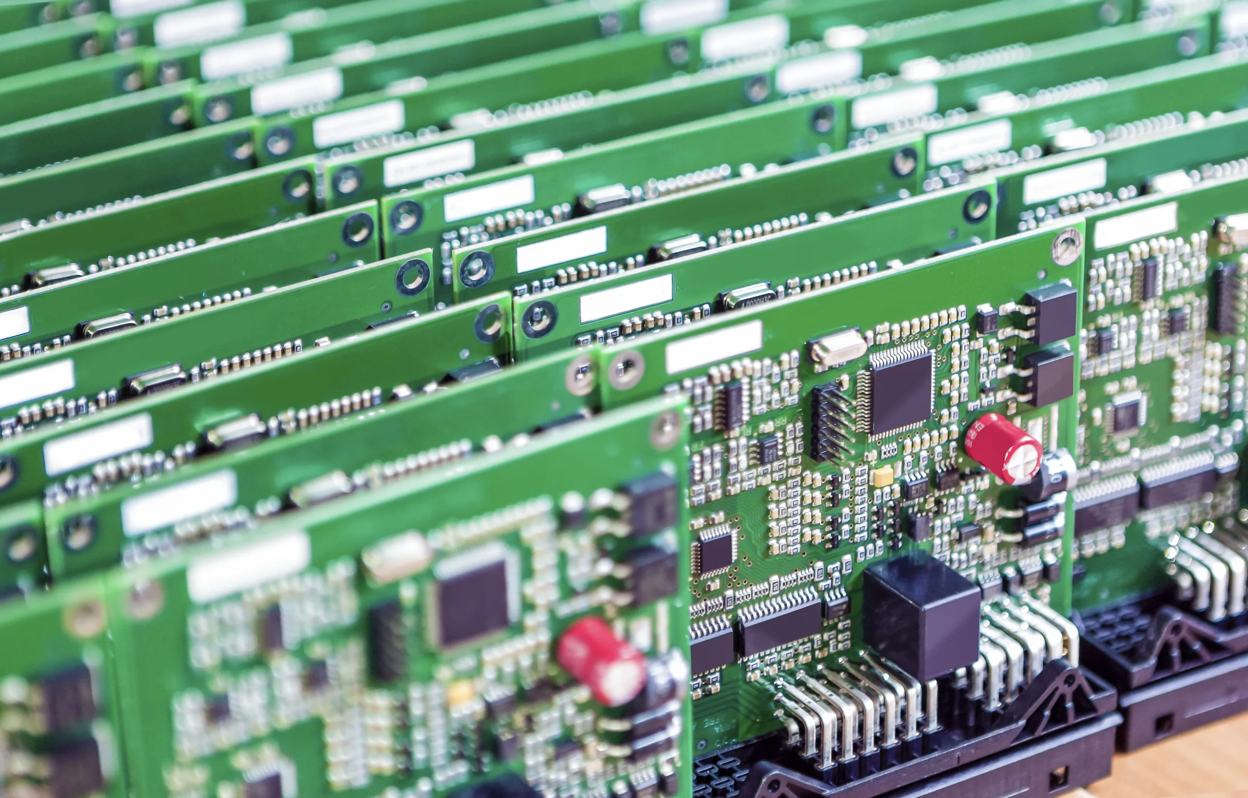
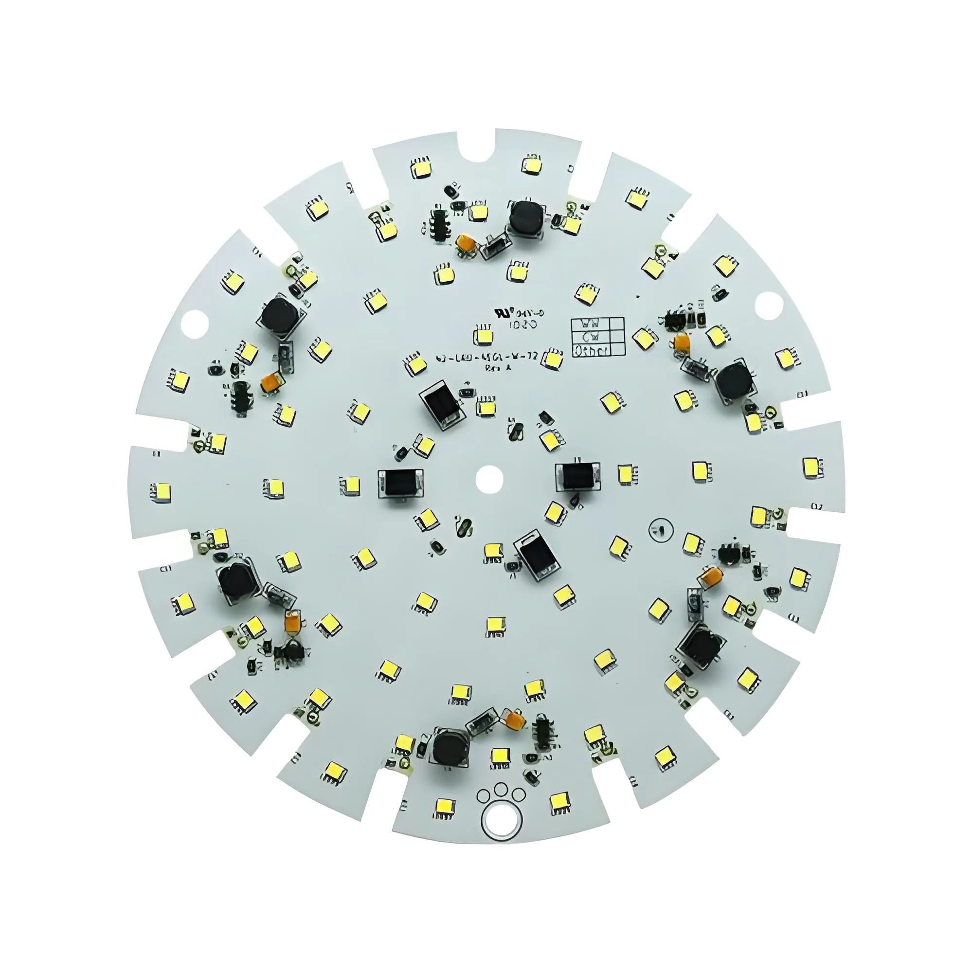
Light LED PCBA Overview
導入
The Light LED PCBA is a compact and efficient printed circuit board assembly designed for LED lighting applications. This PCBA features 1-2 導電性材料の層, making it suitable for simpler circuit designs while maintaining high performance and reliability.
意味
A Light LED PCBA refers to a printed circuit board assembly that incorporates surface mount technology (SMT) or through-hole technology (tht) components specifically for LED lighting applications. The PCBA includes all necessary electronic components soldered onto the PCB, ready for integration into an LED lighting system.
作業原則
The working principle of a Light LED PCBA involves using conductive copper traces on a non-conductive substrate to create electrical pathways. These pathways connect various electronic components such as LEDs, 抵抗器, とコンデンサ. When electrical current flows through these pathways, it powers the LEDs, causing them to emit light.
アプリケーション
This type of PCBA is widely used in various LED lighting applications, 含む:
- Residential and commercial lighting fixtures
- Automotive lighting systems
- Signage and display lighting
- Decorative and architectural lighting
分類
PCBA はいくつかの基準に基づいて分類できます:
- レイヤー数別: 単層, 二重層, または多層 (含む 1-2 レイヤー)
- コンポーネントの種類別: スルーホール, 表面実装, または両方の組み合わせ
- By substrate material: FR-4, アルミニウム, 銅, 等.
材料
The primary materials used in the construction of a Light LED PCBA include:
- 基板: FR-4, アルミニウム, 銅
- 表面処理: HASL鉛フリー / OSP (Organic Solvent Protection)
- Solder Resist: 白
- 銅の厚さ: 0.5オンス~2オンス
- Silk Screen Color: 黒
パフォーマンス
このPCBAの性能の特徴は、:
- 銅層による高い熱伝導率
- 低い信号損失と高い信号完全性
- 湿度や温度の変動などの環境要因に対する抵抗
- RoHS および鉛フリー組立基準への準拠
構造
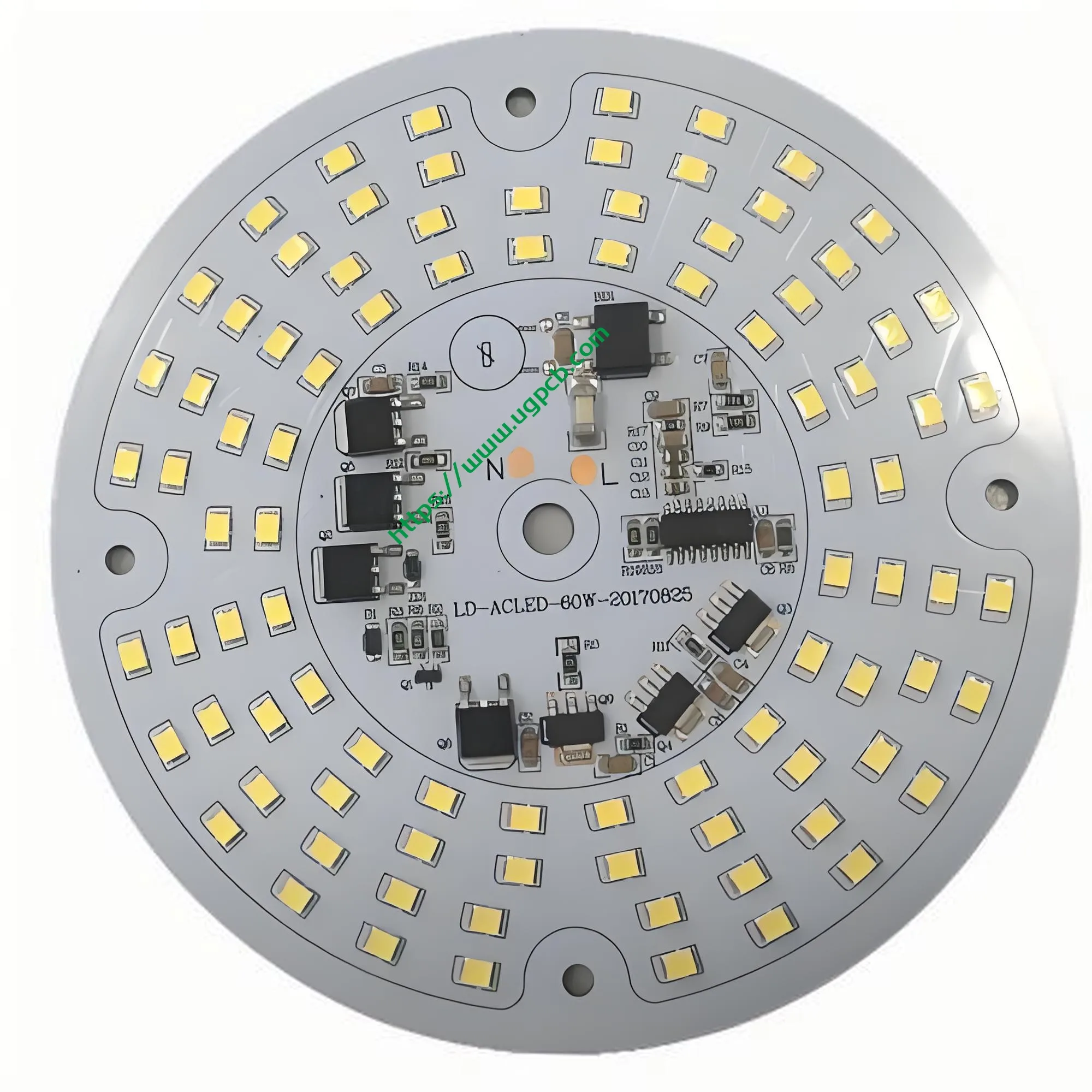
The structure of a Light LED PCBA typically includes:
- Conductive copper traces on a non-conductive substrate
- Surface mount and/or through-hole components soldered onto the PCB
- A white solder mask covering the top layer for protection and identification
- A black silk screen for labeling and component identification
特徴
この PCBA の主な特徴は次のとおりです。:
- Compact and lightweight design suitable for space-constrained applications
- 優れた熱管理機能
- Enhanced durability and longevity in various lighting environments
- Compatibility with a wide range of LED components
製造工程
The production process of a Light LED PCBA involves several steps:
- デザイン: 専用ソフトウェアを使用して回路レイアウトと部品配置を作成.
- 材料の準備: Selecting and preparing the substrate, 銅箔, およびその他の材料.
- レイヤースタッキング: 銅と誘電体材料の層を積み重ねる.
- 掘削を介して: 積み重ねられた層にビア用の穴を開ける (該当する場合).
- メッキ: 電気接続を確保するためにビアを銅でメッキします。.
- エッチング: 過剰な銅を除去して、目的の回路パターンを形成します.
- コンポーネント配置: Soldering surface mount and/or through-hole components onto the PCB.
- テスト: 厳格なテストを実施して、機能と規格への準拠を確認します.
- 最終検査: PCBA がすべての品質および性能基準を満たしていることを確認する.
ユースケース
Common use cases for the Light LED PCBA include:
- Residential and commercial lighting fixtures where energy efficiency and longevity are crucial
- Automotive lighting systems requiring high reliability and performance
- Signage and display lighting in retail and advertising applications
- Decorative and architectural lighting projects needing custom designs and high aesthetics
結論
The Light LED PCBA is an advanced and reliable solution for various LED lighting applications. コンパクトな設計, 高機能素材, and compliance with industry standards make it an ideal choice for engineers and manufacturers seeking efficient and durable electronic solutions.