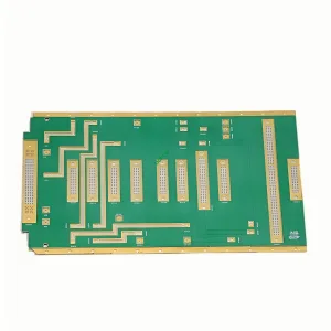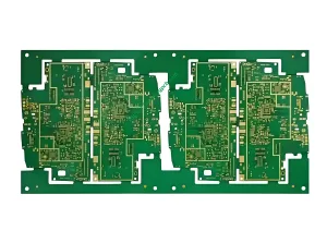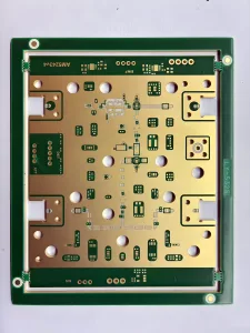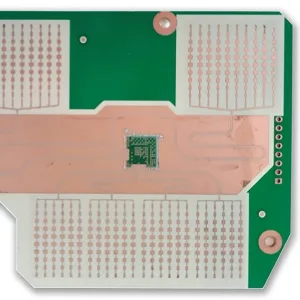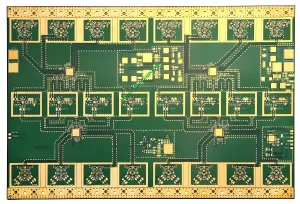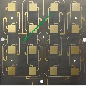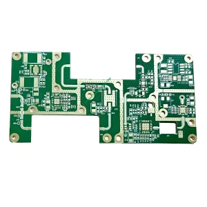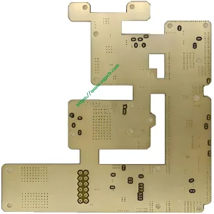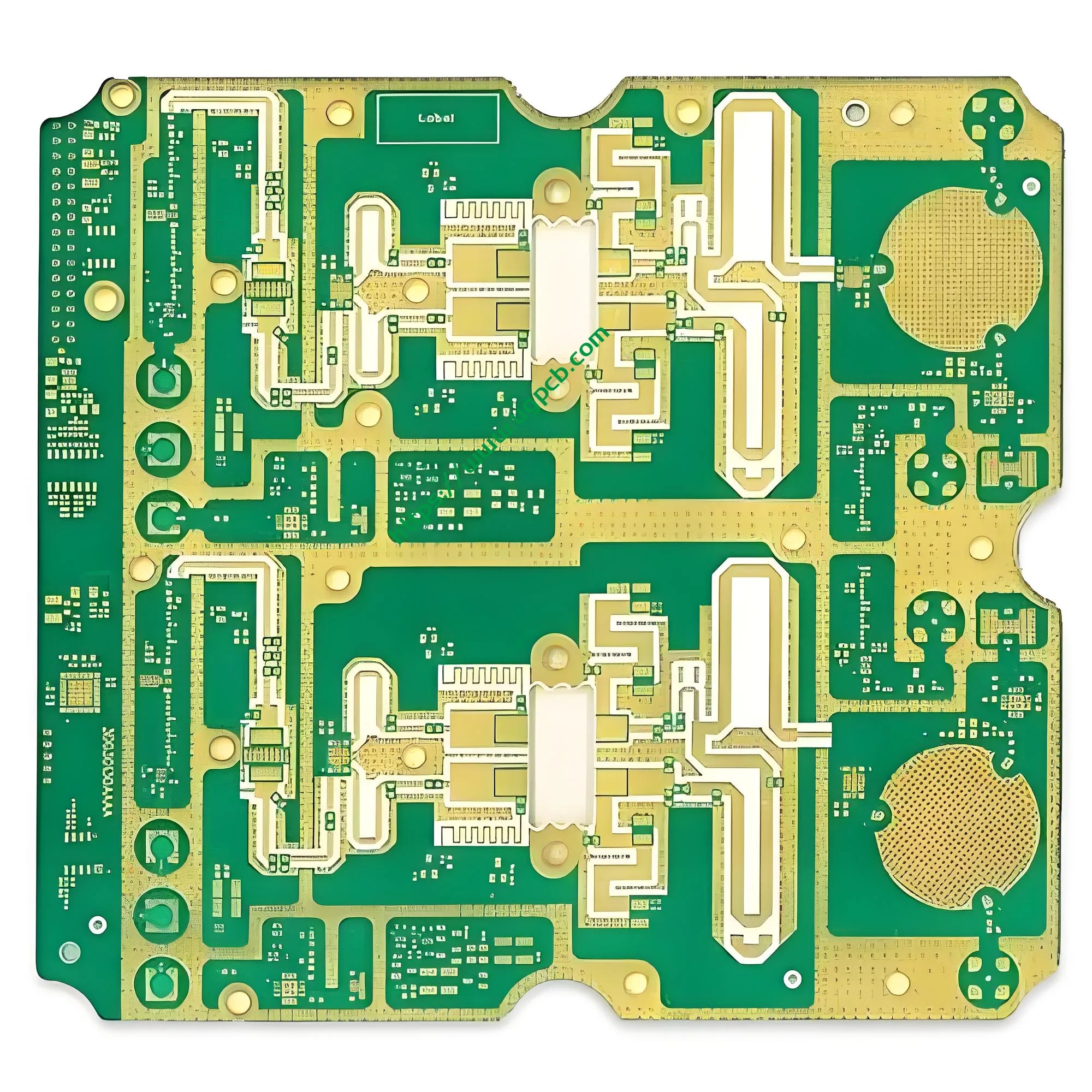
製品の概要
Lightwave Communications PCB Board は、光通信および高速デジタル信号伝送アプリケーション向けに UGPCB によって設計された、プリント基板を介して埋め込まれた高性能 6 層ハイブリッド ブラインドです。. この製品は、ハイブリッドスタックアップを組み合わせた機能を備えています。TU872 高速デジタル素材 とロジャース RO4350B 高周波材. この設計では、高速デジタル信号処理能力と、優れた RF およびマイクロ波信号伝送性能が融合されています。. この PCB は、光通信地上受信装置の理想的な相互接続ソリューションとして機能します。, 高速光トランシーバー, および基地局RFフロントエンドモジュール.
The プリント基板 業界はより高い周波数への取り組みを続けています, より速い速度, そしてより高い密度. 単一材料ソリューションでは、高速デジタル信号と RF アナログ信号という相反する要求を満たすことができなくなりました。. UGPCB は、TU872+RO4350B ハイブリッド設計を通じてこの課題に対処します. この 6 層 PCB は、シグナルインテグリティの最適なバランスを実現します。, 熱管理, そして製造コスト.

製品分類
IPC-6012Eごとリジッドプリント基板の認定および性能仕様, この製品は次のカテゴリに分類されます:
| 分類次元 | カテゴリ |
|---|---|
| 構造タイプ | 多層リジッドプリント基板 (6 レイヤー) ブラインドビアと埋め込みビア付き |
| マテリアルシステム | ハイブリッドラミネート (高速デジタル素材 + 高周波素材) |
| 表面仕上げ | エレクトロレスニッケル/浸漬ゴールド (同意する), IPC-4552用 |
| 信頼性クラス | IPC-6012クラスに適合 2 (専用サービスの電子製品) とクラス 3 (高信頼性電子製品) 要件 |
| 可燃性評価 | UL 94 V-0 |
| アプリケーションドメイン | 光通信 / 通信インフラ用PCB |
主要な技術仕様
| パラメーター | 仕様 |
|---|---|
| レイヤー | 6 レイヤー |
| 材料 | TU872 (高速デジタルレイヤー) + RO4350B (高周波レイヤー) |
| 板厚 | 1.8 mm |
| 銅の厚さ | 35/35/35/35 μm (すべての層に均一に分布) |
| 最小穴径 | 0.20 mm |
| 表面処理 | 同意する (2u” 金の厚さ) |
| 技術的特徴 | 真空栓 + ブラインドビアと埋め込みビア |
主要な材料特性
ロジャース RO4350B 高周波材料 (RF/マイクロ波信号層用):
- 誘電率 (DK): 3.48 ± 0.05 @ 10 GHz
- 損失係数 (Df): 0.0037 @ 10 GHz
- Z軸熱膨張係数 (CTE): 32 ppm/°C
- 可燃性評価: UL 94 V-0
- 熱伝導率: 0.69 w/(m・K)
TU872 高速デジタル素材 (高速デジタル信号層用):
- 誘電率 (DK): < 3.5 @ 10 GHz
- 損失係数 (Df): ~0.009@ 10 GHz
- 高いガラス転移温度 (TG) 優れた熱安定性と耐CAF性を備えています
設計ガイドライン
ハイブリッドスタックアップアーキテクチャ
この 6 層 PCB は、TU872 および RO4350B 材料を使用したハイブリッド スタックアップを採用しています。. 中心となる設計原則の位置付け高周波RF信号伝送を必要とする外層または特定の信号層上のRO4350B, その間TU872 は高速デジタル信号処理層を提供します. この戦略的な材料割り当てにより、単一の PCB で GHz レベルの RF 信号と高速デジタル ロジック信号の両方を処理できるようになります。, 単一材料ソリューションに特有の性能の妥協を排除.
ブラインドおよび埋め込みビアの設計
ブラインドビアは、基板の厚さ全体を貫通することなく、外層を内層に接続します。. 埋め込みビアは完全にボード内に存在します, どちらの外面からも見えない. この 6 層 PCB はブラインドビアおよび埋め込みビア技術を活用して、HDI レベルの配線密度を実現します。.
IPC-6012Eごと, 多層基板 ブラインドビアおよび埋め込みビアを使用する場合は、厳しいめっきおよび充填要件を満たさなければなりません. The 0.20 mm の最小穴直径により、製造歩留まりと高密度配線機能のバランスが取れます。. 6層基板で, 外層から内層へのブラインドビアには、正確な深さの制御が必要です。内層の回路を損傷することなくターゲットの内層まで貫通する必要があります。, 十分な接続面積を確保しながら.
インピーダンス制御設計
信号伝送路の特性インピーダンスは次の式に従います。 (マイクロストリップ構造):
どこ 誘電率です, は誘電体の厚さです, トレース幅です, そして 銅の厚さです. RO4350B の±0.05 という厳しい Dk 許容差により、設計インピーダンス値と製造インピーダンス値の間の偏差が最小限に抑えられます。. この精度は、光通信機器における正確な 50Ω シングルエンドまたは 100Ω 差動インピーダンス制御にとって重要であることがわかります。.
動作原理
信号伝送原理
高周波数で, PCB 信号伝送ラインは次のように機能します。分布定数伝送線路. 誘電率 (DK) 基板の材質が信号の伝播速度を決定します:
どこ 真空中での光の速度です (3×10⁸m/s) そして は実効誘電率です. RO4350Bの低いDk値 (3.48) 約で信号伝播を可能にします 54% 真空中での光の速さ - 従来の FR-4 材料よりも大幅に速い (DK ≈ 4.2-4.8).
損失のメカニズム
PCB 伝送ラインにおける信号損失の合計は次のとおりです。導体損失 そして誘電損失. 誘電損失は材料の誘電正接と直接相関します (Df):
どこ は信号周波数であり、 Dfです. RO4350BのDfはちょうど 0.0037 で 10 GHz では単位長さあたりの誘電損失が極めて低くなります. この特性は、上記の周波数で動作する光通信信号にとって不可欠であることがわかります。 10 GHz.
電気接続による盲目および埋葬
ブラインドビアと埋め込みビアにより、6 層 PCB スタックアップ内の特定の層間の垂直相互接続が確立されます。. スルーホールビアとの比較, 高速信号の完全性を低下させる寄生容量とインダクタンスの影響を大幅に低減します。. この寄生効果の低減は、高速デジタルおよび RF 信号の信号整合性の維持に決定的な影響を与えます。.
製造工程
ハイブリッドラミネートの準備
TU872 と RO4350B のハイブリッド スタックアップは、この製品の主要な製造上の課題を表しています。. これら 2 つの材料は異なる CTE 特性を持っています。RO4350B は、Z 軸の CTE を示します。 32 ppm/°C, 一方、修飾エポキシ系としての TU872 は異なる熱機械特性を持っています。. UGPCB は、正確な積層パラメータ制御により、信頼性の高いハイブリッド界面の接合と強度を実現します (温度プロファイル, 圧力プロファイル, およびランプレート).
ブラインドおよび埋め込みビア製造
- 地層を介して埋められた: 内層コアは積層前に穴あけと銅メッキが施されます, 基板内の埋め込みビアをカプセル化する
- ブラインドビアの形成: ラミネート後, 外層からの制御された深さの穴あけは、正確な深さ制御で指定された内層をターゲットにします
真空栓抜き工程
IPC-4761 によるプリント基板ビア構造の保護設計ガイド, 真空プラグはビア保護タイプ VI に該当します (完全に充填してカバーする) またはタイプVII (完全に埋める) カテゴリ. 主要なプロセスパラメータ:
- プロセスフロー: 穴あけ → デスミア →真空栓抜き → 硬化 → 研磨
- プラグ充填率: ≥ 85% (IPC-6012 要件に準拠)
- 真空環境によりビアホール内の気泡が除去されます。, ブラインドビアおよび埋め込みビアの完全な樹脂充填を保証します。
表面仕上げ (同意する)
エレクトロレスニッケル/浸漬ゴールド (同意する, 2u” 金の厚さ) 表面仕上げはIPC-4552仕様に準拠:
- 無電解ニッケル層: 3-6 μm
- 浸漬金層: ≥ 0.05 μm (2u” ≈ 0.05 μm)
- ENIG は平らなはんだ付け可能な表面を提供します, 優れたはんだ付け性, そして長い保存期間
性能特性
信号の完全性 (そして) 利点
- 低挿入損失: RO4350Bの低いDf (0.0037@10 GHz) 伝送中の高周波信号のエネルギー損失を最小限に抑えます
- 低い誘電率の変化: わずか ±0.05 の Dk 許容差により、インピーダンスの一貫性が保証されます
- 安定した電気的性能: TU872 は、さまざまな温度と湿度の条件下でも電気的特性を維持します
熱管理性能
- 1.8 mm の板厚により、優れた熱質量と機械的強度が得られます。
- RO4350Bの熱伝導率 0.69 w/(m・K) 効果的に熱を放散します
- TU872 の高い Tg により、高温での寸法安定性が保証されます
信頼性
- 真空プラグによりボイドのないブラインドビアと埋め込みビアが保証されます, IPC-6012クラスに適合 2/3 要件
- ユニフォーム 35 4 つの層すべてにわたる μm の銅の厚さにより、通電容量と熱放散が確保されます。
- UL 94 V-0 可燃性評価 - 炎は以下の範囲内で消火します。 10 取り外してから数秒後
アプリケーションシナリオ
地上受信設備
これは、プライマリターゲットアプリケーション この商品について. 地上受信装置は、衛星またはマイクロ波リンクからの高周波 RF 信号を同時に処理する必要があります。 (RO4350B 材料が必要) およびベースバンドデジタル信号処理 (TU872 材料が必要). この6層は ハイブリッド基板 この二重の要件に正確に対応します.

光通信システム
- 光ファイバーネットワーク伝送装置
- 光トランシーバー
- 光増幅器
高速デジタル通信
- 5G通信基地局RFフロントエンド
- 高速データ交換装置
- 試験および測定機器
UGPCBを選択する理由?
- 成熟したハイブリッドラミネート技術: 制御可能な歩留まりを備えたTU872+RO4350Bハイブリッドスタックアップによる広範な生産経験
- 高度なブラインドおよび埋め込みビア機能: 0.20 真空プラグによる最小穴径 mm は HDI 相互接続要件を満たします
- エンドツーエンドの品質制御: 材料の受け入れから完成品の出荷までの全プロセスの品質管理, 厳密に IPC-6012E 規格に準拠
- 迅速な応答: 専門のエンジニアリングチームが DFM を提供します (製造可能性のための設計) レビューサポート
お問い合わせのご案内
サンプルを入手するには, ボリュームプライシング, またはライトウェーブ通信 PCB ボードのテクニカル サポート, 提供してください:
- ガーバーファイル (スタックアップの詳細を含む)
- BOMリスト (PCBA サービスが必要な場合)
- 特別なパフォーマンス要件 (インピーダンス値, テスト仕様書, 等)
UGPCB のチームは、専門的な技術評価と見積もりを以内に提供します。 24 時間.
データソース宣言
この文書で引用されている技術データと規格は、次の信頼できる情報源から得られています。:
- ロジャースコーポレーション – RO4350B™ ラミネート データシート
- IPC (エレクトロニクス産業をつなぐ協会) – IPC-6012E リジッドプリント基板の認定および性能仕様; IPC-4761 プリント基板ビア構造の保護のための設計ガイド; IPC-4552 無電解ニッケル/浸漬金の性能仕様 (同意する) プリント基板用めっき
- UL (引き受けの研究所) – UL 94 機器・家電部品のプラスチック材料の燃焼性試験に関する規格
- 太陽テック (TUC) – TU-872 SLK ハイスピード材技術データ