

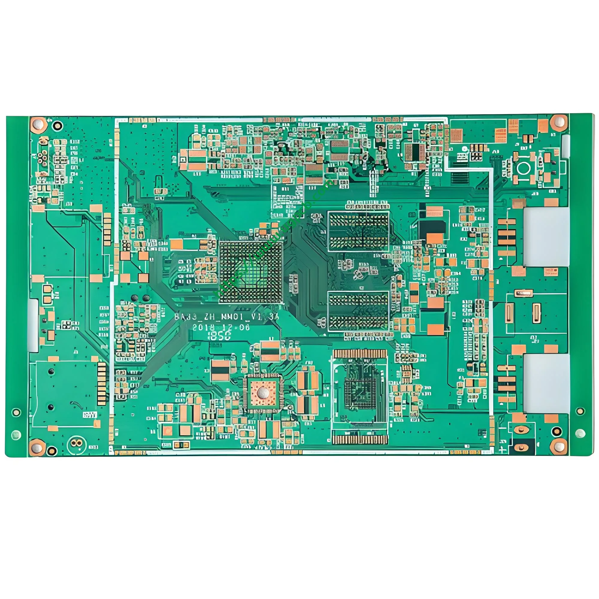
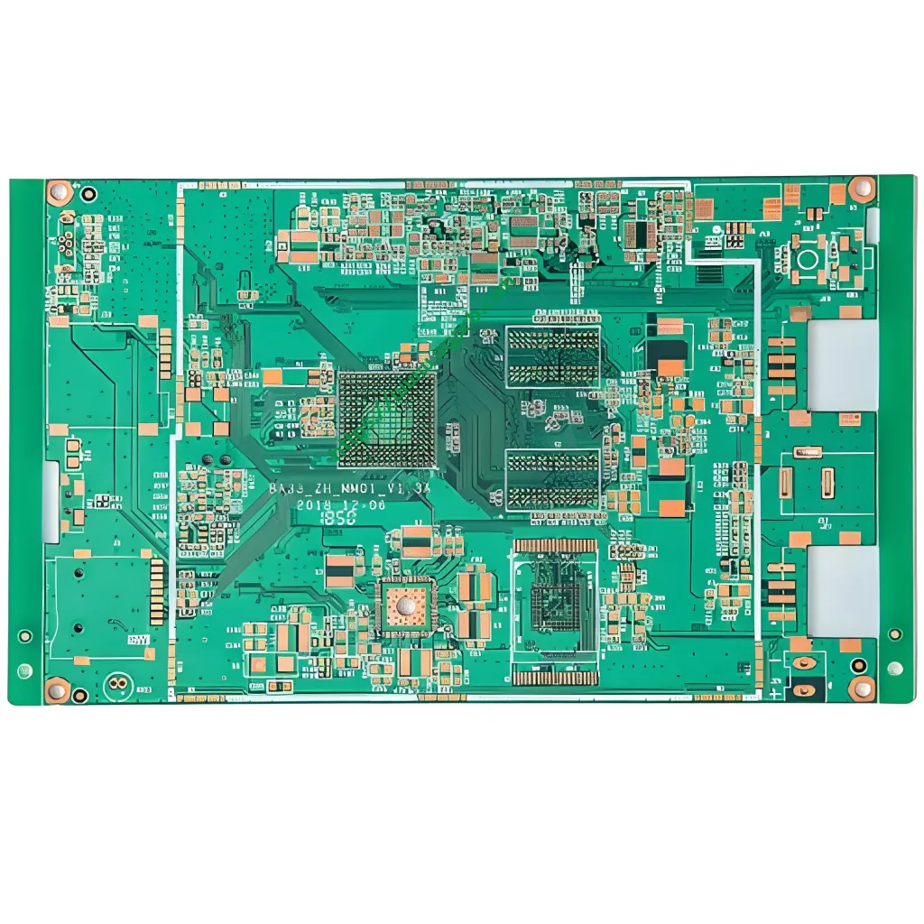
製品の概要: OSP 酸化防止 PCB 回路基板とは?
アンOSP酸化防止PCB回路基板 用途有機はんだ付け性保存剤 (OSP) 銅の表面仕上げとして. このプロセスでは、裸の銅表面に極薄の有機膜を堆積します。. フィルムは保管時や組み立て時の酸化を防ぎます。. はんだ付け時, フラックスはOSPフィルムを急速に溶解します. これにより、信頼性の高いはんだ接合のためにきれいな銅が露出します。.
UGPCB の OSP 酸化防止剤 PCB 回路基板は使用していますFR-4 ガラスエポキシ積層板 基材として. 35μmが特徴です (1 オンス) 銅箔, 1.6板厚mm, と寸法 68.36 ×34.6mm. 最小仕上げ穴サイズは0.45mmです. 最小トレース幅は0.15mm、最小間隔は0.20mm. この製品はIPC-6012Eに完全に準拠しています。 (リジッドプリント基板の認定と性能) および IPC-4555 (高温OSP性能) 仕様.
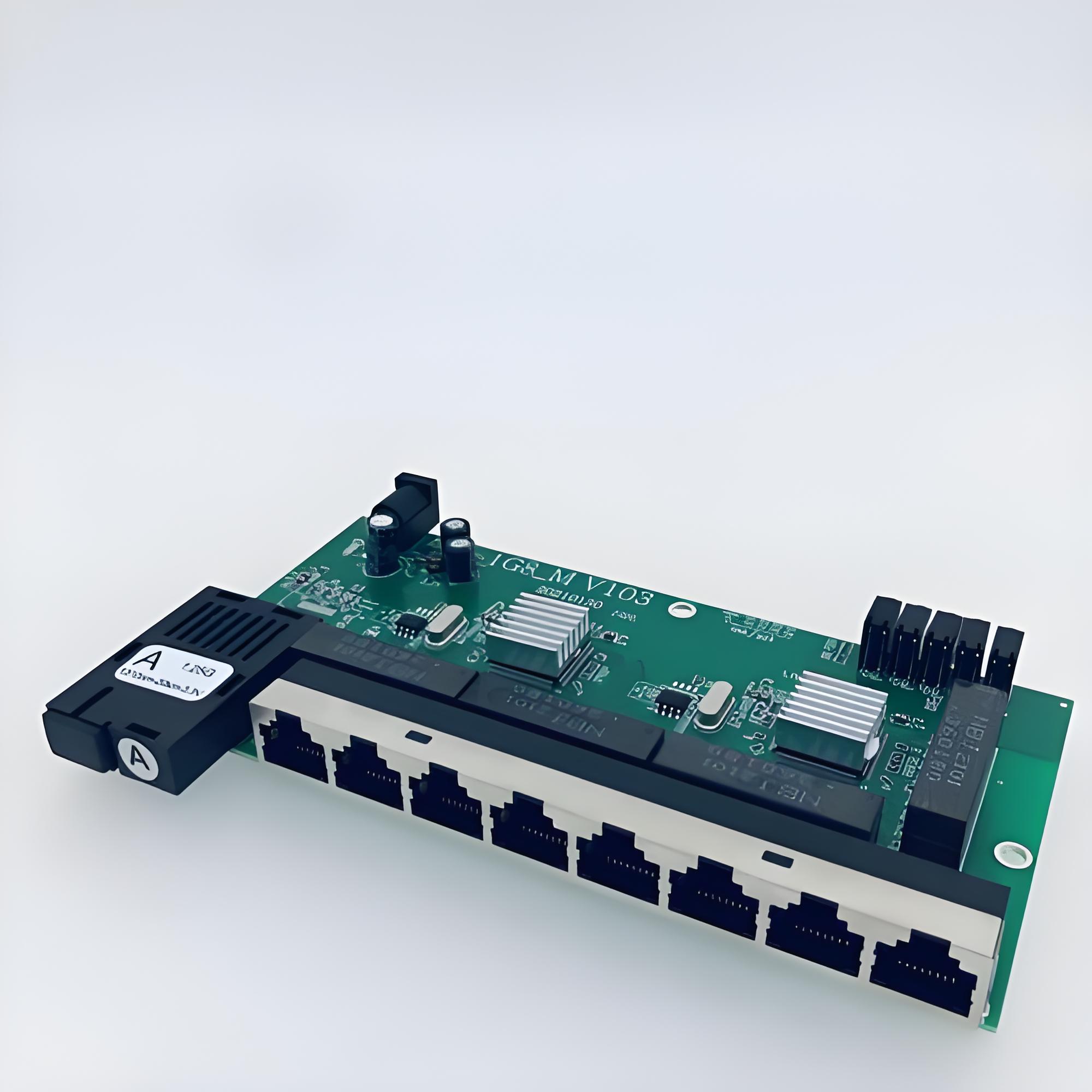
これ両面OSP PCB 家庭用電化製品を提供する, 通信機器, および産業用制御. コスト重視と表面の平坦性が最も重要な場合に最適に機能します。.
科学製品の分類
国際的な PCB 分類システムに基づく, この製品は次のカテゴリに分類されます:
| 分類次元 | カテゴリ |
|---|---|
| 基板材料 | FR-4 エポキシガラス布リジッド PCB |
| レイヤー数 | 両面 (2層回路) |
| 表面仕上げ | OSP (有機はんだ付け性保存剤) 抗酸化物質 |
| 可燃性評価 | UL 94 V-0 |
| IPCパフォーマンスクラス | クラス 2 (専用サービスの電子製品) |
| 銅箔の厚さ | 1 オンス (35μm) 標準銅 |
| 板厚 | 1.6mm標準リジッドボード |
| 穴タイプ | SMT対応スルーホール |
主要な技術パラメータの説明
基板: FR-4 エポキシガラス生地
FR-4 は、最も一般的なリジッド基板です。 プリント基板 業界. “フランス” 難燃性を意味します. “4” は、エポキシ樹脂とガラス繊維を組み合わせたものを指します。UL 94 V-0 可燃性基準. UL 94 V-0 内部で自己消火するには垂直の試験片が必要です10 秒 10秒間の炎を2回当てた後. 燃えるような滴りが綿に発火する可能性はありません.

ガラス転移温度 (TG) 耐熱性を測る. 標準 FR-4 Tg 範囲は 130 ~ 140°C. 中Tg FR-4は150~160℃に達します. 170℃を超える高Tg FR-4. この製品は、Tg ≥ 130°C の標準 FR-4 を使用しています。 (IPC-4101/21準拠). リフローはんだ付けの熱衝撃要件を満たします。 (ピーク温度 240 ~ 260°C).
銅箔の厚さ: 35μm (1 オンス)
銅の厚さによって電流容量が決まります. この製品が使用しているのは、35μm 銅箔, として知られている1 oz銅 (1 オンス/平方フィート ≈ 35μm). IPC-2221によると, 1 10℃の温度上昇でオンスの銅は約:
- 0.15mm (6 ミル) トレース幅: 0.5-0.7A
- 0.20mm (8 ミル) トレース幅: 0.8-1.0A
銅の厚さ 35μm は、両面 PCB の最も一般的な標準です。. コストのバランスが取れている, 電流容量, および製造歩留まり.
基板寸法: 68.36 ×34.6mm
完成したボードの寸法68.36mm×34.6mm. このコンパクトなサイズは、狭い電子モジュールに適しています. 小型 PCB ではより厳しい精度が要求され、寸法公差は通常 ±0.15mm 以内に収まります。 (IPC-6012クラス 2).
最小仕上げ穴サイズ: 0.45mm
0.45mm 最小のメッキスルーホールです (PTH) 直径. この穴のサイズは業界の標準です. 確実なめっきを保証します (アスペクト比はおよそ 3.6:1 板厚1.6mm). 穴のサイズは、ほとんどの DIP コンポーネントと標準的な SMT パッド設計に対応します。.
プリント基板の厚さ: 1.6mm
1.6mm PCB製造において最も一般的な板厚です。. 優れた機械的強度と曲げ剛性を備えています。. 標準のコネクタとソケットに完全に適合します.
トレース幅と間隔: 0.15mm / 0.20mm
この製品が提供するのは、最小トレース幅0.15mm (について 6 ミル) そして最小間隔0.20mm (について 8 ミル). IPC分類によると, これらの次元は以下に分類されますクラス 2 (専用サービスの電子製品). この精度は、ほとんどの中密度 PCB 設計に適合します。, MCU制御ボードを含む, 電源管理モジュール, およびインターフェースコンバータボード.
OSP 抗酸化プロセスの仕組み
OSP プロセスは、きれいな裸銅上に極薄の有機膜を成長させます。化学吸着. OSP フィルムの主な構成要素は、アルキルベンズイミダゾール化合物 (アゾール系). フィルムの厚さは通常、次の範囲です。0.2–0.5μm.
保護メカニズム
OSP フィルムは 3 つのメカニズムで銅表面を保護します。:
- 物理的バリア – 有機膜は緻密な分子層を形成します. 酸素や水分が銅表面に接触するのを防ぎます。.
- 化学吸着 – OSP分子の活性基が銅原子と化学結合する. これにより強力な接着力が得られます.
- 選択的保護 – OSP フィルムは銅領域のみをカバーします. ソルダーマスクや他の非金属領域には影響しません。.
はんだ付け時の動作
SMTリフロー時, 到達温度190–230℃. フラックスの有効成分がOSP膜を分解・溶解します。. これにより、その下のきれいな銅が露出します. はんだは裸の銅に直接接触して形成されます。金属間化合物 (IMC). これにより、信頼性の高い電気接続が確立されます。. OSPフィルム完全に分解する はんだ付け後に残留物が残らない.
主なパフォーマンス特性
IPC-TM-650 試験方法に基づく:
| 特性 | 代表値 / 要件 | 参照標準 |
|---|---|---|
| OSP膜厚 | 0.2–0.5μm | IPC-4555 |
| はんだ濡れ角 | ≤30° (後 1 リフロー) | IPC-TM-650 2.4.1 |
| はんだ広がり率 | ≥80% | IPC-TM-650 2.4.1 |
| 酸化防止 (アンビエント) | 6か月以上 | IPC-4555 |
| 接触抵抗の変化 | ≤10% (後 6 数カ月の保管) | IPC-TM-650 |
OSP 酸化防止剤 PCB の製造プロセス
OSP 酸化防止剤 PCB の製造は厳格なプロセス管理に従って行われます. あらゆるステップが最終的な品質と信頼性に影響を与えます.
フロントエンドプロセス (基板の準備 & 回路パターニング)
- 材料の切断 – FR-4 銅張積層板をサイズに合わせてカットします
- 掘削 – 最小穴サイズ0.45mmのCNCドリル加工
- 無電解銅 / 電気めっき – 層間の接続のために穴の壁を金属化する
- 回路パターン転写 – ドライフィルム / ウェットフィルムの露光と現像
- エッチング – 不要な銅を除去して0.15mmのトレースを作成します / 0.20mm間隔の回路
- ソルダーマスク印刷 – 緑色または他の色のソルダーマスクインクを塗布します
- プレクリーン – 表面仕上げの前に酸化物や汚染物質を除去します。
OSPコーティングプロセス (コアプロセス)
典型的なOSPコーティングフロー:
脱脂 → 2回水洗 → マイクロエッチング → 2回水洗 → 酸洗 → 純水リンス → OSP 成膜 → 風乾 → 純水リンス → 最終乾燥
- マイクロエッチング – 酸化銅を除去し、均一で微細な粗い表面を作成します。. これによりOSP膜の成長が促進されます.
- OSP膜形成 – PCB を OSP 化学薬品に浸す (アルキルベンジミダゾール, 有機酸, 塩化銅, 脱イオン水). 銅表面への化学吸着により膜が成長します。.
- 膜厚制御 – 正確な制御が重要です. 薄すぎると耐熱性が低下します. 厚すぎるとフラックスの作用とはんだの流れが妨げられます.
バックエンドプロセス
- ルーティング – 最終寸法への CNC ルーティング
- 電気テスト – フライングプローブまたはフィクスチャのテスト
- 最終検査 – 目視検査と膜厚サンプリング
- 真空包装 – 防湿・耐酸化包装
製品の特徴と主な利点
優れた表面の平坦性
OSPフィルムは0.2–0.5μm 厚い. 化学吸着により形成され、厚みが均一で表面が滑らかです。. これにより、元の銅箔の平坦性が維持されます。. に最適ですファインピッチSMT コンポーネント (0.4mm以下ピッチQFPなど, QFNパッケージ).
優れたはんだ付け性
OSP フィルムはリフロー中にフラックスにすぐに溶解します。. これにより、信頼性の高い IMC 形成のために新鮮な銅が露出します。. OSP プロセスは両方をサポートしますスルーホール (tht) そして表面実装 (SMT) はんだ.
費用対効果が高い
OSPは貴金属を使用していません (金, 銀, パラジウム). 材料費と加工費がENIGより安い, 浸漬シルバー, または浸漬錫. 家電製品などの大量生産向け, OSP は優れたコスト競争力を提供します.
環境に適合
OSPは有機化合物を使用しています. 鉛は含まれていません, 水銀, カドミウム, または六価クロム. 完全に満たしてるよRoHS 2.0 要件. 廃棄物処理のコストと複雑さも金属仕上げプロセスよりも低くなります.
短い処理時間
OSP コーティングはシンプルかつ迅速です. 複雑なメッキ装置や長い蒸着時間は必要ありません。. ENIGとの比較 (何時間もかかります), OSPは表面仕上げを完了します30-60分 バッチごと. これによりリードタイムが大幅に短縮されます.
設計ガイドラインと重要な考慮事項
製造用のデザイン (DFM) ルール
この製品のプロセス能力に基づく:
| 設計パラメータ | 製品の機能 | 推奨設計値 |
|---|---|---|
| 最小トレース幅 | 0.15mm | ≧0.15mm (信号トレース) |
| 最小間隔 | 0.20mm | ≧0.20mm |
| 最小穴サイズ | 0.45mm | ≧0.45mm |
| 板厚 | 1.6mm | 1.6mm (標準) |
OSP プロセスの制限と緩和策
OSP には多くの利点がありますが、固有の制限があります:
- 有効期限が限られている – OSP フィルムが保護します6 月 周囲条件で. 最高のはんだ付け性を実現, 以内に SMT アセンブリを完了する 3 月.
- 耐湿性 – OSP フィルムは高温で劣化します, 高湿度環境. ボードを次の場所に保管します20–25°C、相対湿度 40 ~ 60%.
- 限られたリフローサイクル – 標準 OSP 耐性1–2 リフロー熱衝撃. 複数のリフローには高温 OSP が必要です (IPC-4555準拠).
- 電気試験の課題 – OSPフィルムは絶縁性です. 電気テストの接触信頼性に影響します. OSP 層を除去するには、テスト ポイントにはんだペーストの印刷が必要です.
保管と取り扱いに関する推奨事項
- 乾燥剤と湿度インジケーターカードを備えた真空密封パッケージ
- 保管環境: 温度≤30°C, 相対湿度 ≤60%
- 内で半田付け完了48 時間 パッケージを開けたところ
- 取り扱い中は静電気防止手袋を着用してください. 素手でボード表面に触れないようにしてください.
典型的なアプリケーションシナリオ
OSP 酸化防止 PCB 回路基板は、その特性により多くの産業に貢献しています。コストメリット, 表面の平坦度, 優れたはんだ付け性:
家電
- スマートフォンのマザーボードとタブレットのPCB
- コンピューターのマザーボードとグラフィックス カード
- 家電制御盤
- ウェアラブルデバイスの回路基板
通信機器
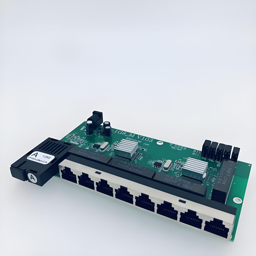
- ルーターとスイッチの PCB
- 通信モジュールとIoTデバイス
- ブルートゥース / Wi-Fiモジュールキャリアボード
産業用制御
- PLCプログラマブルロジックコントローラー
- 電源管理モジュール
- 計装回路基板
- モータードライブ制御基板
カーエレクトロニクス (安全性が重要ではない)
- 車載インフォテインメント システム
- ボディコントロールモジュール
- センサーインターフェースボード
品質保証と規格準拠
適用規格
UGPCB の OSP 酸化防止剤 PCB 製品は、これらの国際規格に厳密に従っています:
| 標準 | タイトル | 範囲 |
|---|---|---|
| IPC-4555 | 高温有機はんだ付け性防腐剤の性能仕様 (OSP) プリント基板用 | OSP プロセスの要件とテスト |
| IPC-6012E | リジッドプリント基板の認定および性能仕様 | 完成したボードの品質とパフォーマンス |
| IPC-4101/21 | ガラス強化エポキシ積層板の仕様 | FR-4 基板の技術要件 |
| IPC-TM-650 | 試験方法マニュアル | 各種性能試験方法 |
| UL 94 V-0 | プラスチック材料の可燃性 | 基材の難燃性の安全性 |
| RoHS 2.0 | 有害物質の制限 | 環境コンプライアンス |
主要な品質指標
IPC 要件ごと, 主要な品質指標には以下が含まれます:
- OSP膜厚: 0.2–0.5μm, 均一性公差 ≤ ±0.1μm
- 接着力: 4B以上 (IPC-TM-650 2.4.29 クロスカットテスト)
- はんだ広がり率: ≥80% (IPC-TM-650 2.4.1)
- 酸化防止期間: 6か月以上 (周囲条件)
- 可燃性評価: UL 94 V-0
OSP 酸化防止 PCB に UGPCB を選択する理由?
精密製造能力
- 0.15mm 最小トレース幅 / 0.20mmの最小間隔
- 0.45mm 最小仕上げ穴サイズ
- 1.6互換性に優れたmm標準板厚
信頼性の高いOSPプロセス制御
- 膜厚と品質については IPC-4555 に厳密に準拠
- 製造プロセス全体にわたる完全なトレーサビリティ
- バッチごとのはんだ付け性試験と膜厚サンプリング
迅速な配達
- 標準リードタイム: 7–10営業日
- 試作サンプリングと量産の両方に対応
包括的な技術サポート
- 無料の DFM 設計レビュー
- 製品選択のガイダンスを提供する専門のエンジニアリングチーム
今すぐ見積もりを入手
UGPCB は、高価値の OSP 酸化防止剤 PCB 回路基板ソリューションを提供します. 必要かどうかプロトタイプのサンプリング または量産, 専門的な技術サポートと競争力のある価格を提供します.
📞 見積もりの入手方法:
- ガーバーファイルとBOMリストを送信してください
- 当社のエンジニアリング チームは、カスタマイズされたソリューションと見積もりを提供して対応します。24 時間
- 無料の DFM チェックにより、デザインが最初に合格することを確認します
データソースステートメント: この文書で引用されている技術データと標準要件は主に IPC から得られたものです。 (エレクトロニクス産業をつなぐ協会) IPC-4555を含む規格 “高温有機はんだ付け性防腐剤の性能仕様 (OSP) プリント基板用,” IPC-6012E “リジッドプリント基板の認定および性能仕様,” IPC-4101/21 “ガラス強化エポキシ積層板の仕様,” IPC-TM-650 “試験方法マニュアル,” およびUL 94 “機器や家電製品の部品に使用されるプラスチック材料の燃焼性試験の規格。” 一部のプロセスパラメータは、大手 PCB メーカーから公開されている技術データを参照しています。. すべてのデータは正確であることが検証されています.













