What are PCB terminals?
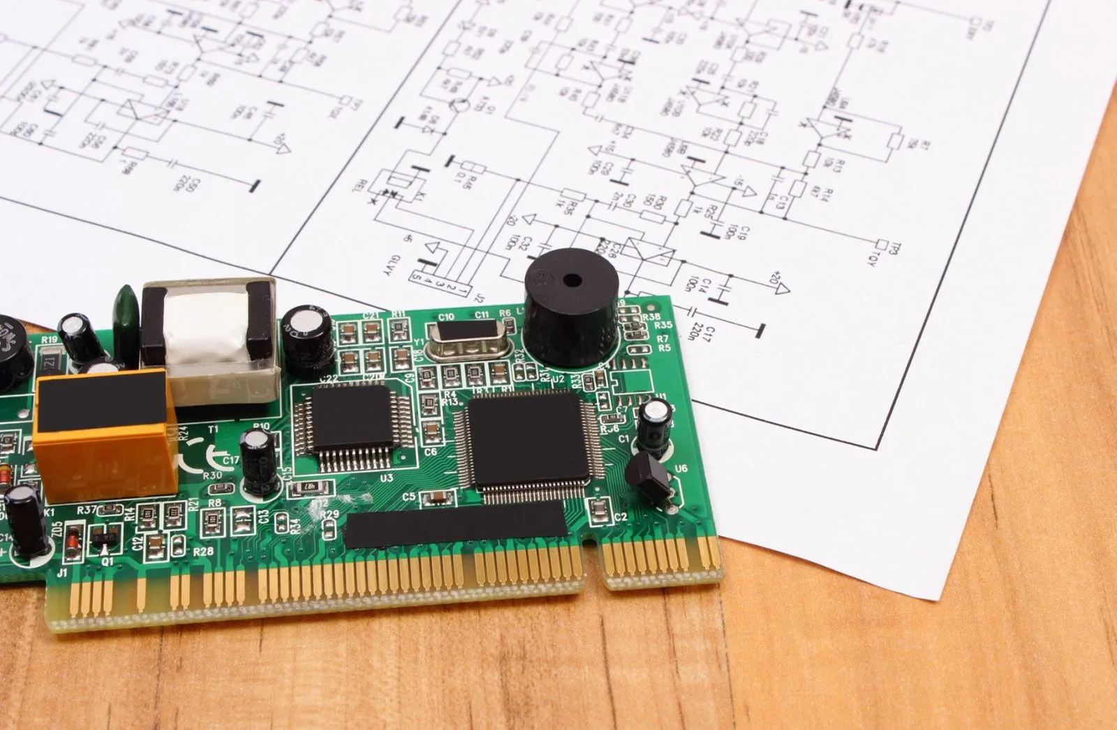
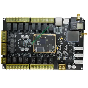
PCB terminal blocks are modular insulating devices that mount on a printed circuit board (プリント基板) and hold two or more wires together. Terminal blocks are used to hold and/or terminate electrical wires and in their simplest form consist of multiple individual terminals arranged in long strips.
PCB terminal blocks make it easy and safe to transfer signals, data and power to the PCB. They are suitable for a wide variety of applications in numerous industries, markets and Industry 4.0 アプリケーション. Our COMBICON range of XS to XXL product lines includes metric and imperial pitch, from 2.5mm pitch miniature terminals to 20mm pitch power stage terminals.
 UGPCBのロゴ
