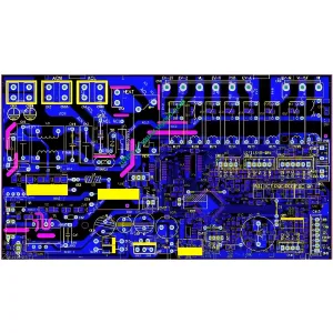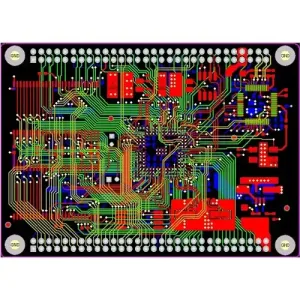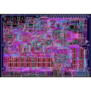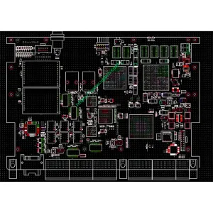
1. 製品の概要
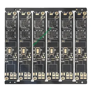
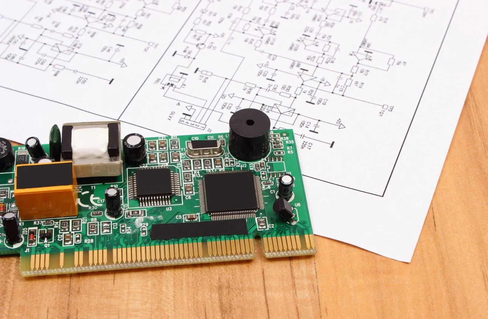
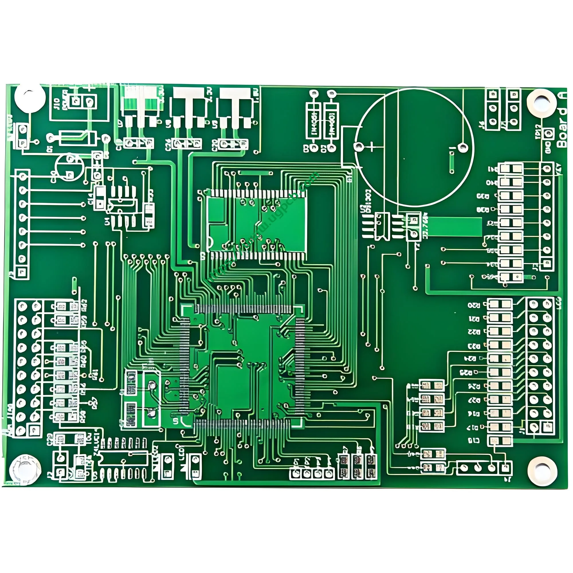
あserver power backplane PCB is a critical interconnect component in server power systems. It distributes electrical energy from power supply modules to server motherboards, hard drive backplanes, and expansion cards. This board does not have onboard storage or processing power. スロットのあるボードはマザーボードではなくバックプレーンと呼ばれます.
UGPCB offers this server power backplane PCB with the Kingboard KB6167F high-Tg lead-free laminate. The board has a 1.6mm thickness, 2 レイヤー (両面), and a compact 78.26×61.3mm form factor. It meets IPC-6012 Class 2 パフォーマンス要件. The product uses Lead-Free Hot Air Solder Leveling (出血) as the surface finish.

2. 製品分類
これ server PCB falls into the following categories per IPC標準:
| 分類 | カテゴリ |
|---|---|
| 構造によって | Rigid Double-Sided PCB (2-層) |
| アプリケーションによって | Server Power Backplane – Computer & Peripheral Equipment |
| パフォーマンスクラス別 | IPC-6012クラス 2 – Dedicated Service Electronic Products |
| By Substrate | FR-4 Flame-Retardant Epoxy Glass Cloth Laminate (UL 94 V-0) |
| 表面仕上げによる | 鉛フリー熱風はんだレベリング (鉛フリーHASL) |
| By Solder Mask / 伝説 | Green Solder Mask with White Silkscreen |
3. 主要な技術仕様
3.1 基板: Kingboard KB6167F High-Tg Lead-Free Laminate
KB6167F is a high-performance FR-4 laminate from Kingboard Holdings Limited. It belongs to the high-Tg lead-free epoxy copper clad laminate series.
| パラメーター | 代表値 | 試験規格 |
|---|---|---|
| ガラス転移温度 (TG) | ≥170°C (DSC法) | IPC-TM-650 |
| 熱分解温度 (TD) | >340℃ | IPC-TM-650 |
| 可燃性評価 | UL 94 V-0 | UL規格 |
| Primary Specification | IPC-4101/126 | IPC-4101 |
TheTg of ≥170°C allows the material to withstand lead-free reflow soldering at peak temperatures of260℃. Standard Tg materials (130–140℃) risk delamination during multiple reflow cycles. KB6167F also offerslow Z-axis CTE and excellentカフェ抵抗.
3.2 板厚: 1.6mm
The 1.6mm thickness provides adequate mechanical strength for connector insertion. It also enables mature, stable processing with high yield rates.
3.3 レイヤー数: 2 レイヤー (両面)
Power backplanes focus on power distribution rather than high-speed signal routing. The 2-layer design delivers lower cost, shorter lead times, and higher reliability compared to multilayer boards.
3.4 寸法: 78.26 × 61.3mm
This compact size fits standard 1U or 2U server chassis spaces. UGPCB offers flexible customization for different chassis configurations.
3.5 最小穴の直径: 0.281mm
The aspect ratio determines plated through-hole reliability:
アスペクト比 = 基板の厚さ / Minimum Hole Diameter = 1.6mm / 0.281mm ≈ 5.69:1
This ratio is well below the industry standard10:1 upper limit. UGPCB applies70 minutes of pattern plating to achieve hole copper thickness of18–22μm. IPC-6012クラス 2 requires a minimum of20μm on plated through-hole walls.
3.6 線幅 / 行間: 0.21 × 0.186mm
The minimum line width of0.21mm (約. 8.3 ミル) and minimum spacing of0.186mm (約. 7.3 ミル) meet precision circuitry requirements per IPC-2221C.
3.7 銅箔の厚さ: 1/1 オズ
Both layers have1 オンス (約. 35μm) 銅箔. A 0.21mm-wide trace on 1OZ copper carries approximately1.5–2A at 10°C temperature rise per IPC-2221 calculations.
3.8 表面仕上げ: 鉛フリー熱風はんだレベリング
Lead-Free HASL usesSAC305 alloy (Sn-3.0Ag-0.5cu). Key advantages include:
- RoHS compliance
- 優れたはんだ付け性
- Extended shelf life (>12 months)
- Cost-effective for high-volume production
This finish complies withIPC-4554.
3.9 はんだマスク / 伝説: Green Oil / White Character
Green solder mask provides excellent insulation and high-temperature resistance. White silkscreen ensures clear component identification for PCBA assembly and maintenance.
4. 設計上の考慮事項
4.1 Power Integrity Design
Power integrity is the primary design focus for aserver power backplane PCB. Key elements include:
- Low-impedance Power Distribution Network (PDN) with large power and ground planes
- Adequate current-carrying capacity based on server power module output
- Voltage drop control from input to output ports
4.2 熱管理
High-current transmission generates significant heat. The design addresses this through:
- High-Tg material selection (KB6167F Tg≥170°C)
- Optimized heat dissipation paths with strategic copper layouts and thermal vias
4.3 製造可能性のための設計 (DFM)
Per IPC-2221 and IPC-2222:
- アスペクト比 5.69:1 – well below the 10:1 industry limit
- Minimum line width 0.21mm – mature etching process for 1OZ copper
- Dimensional tolerances: CNC routing ±0.15mm (6 ミル), steel die punching ±0.10mm (4 ミル)
5. 動作原理
Theserver power backplane PCB operates through three functional layers:
Power Input Layer: Power supply modules deliver DC power (typically 12V or 48V) through input connectors.
Power Transmission Layer: Electrical energy travels through carefully designed copper traces (電源層とグランド層). 銅の厚さ (1オズ) and trace widths ensure safe temperature rise at rated currents.
Power Output Layer: Distributed power reaches output connectors that supply the server motherboard, hard drive backplanes, 拡張カード, and other functional modules.
6. アプリケーションとユースケース
| 応用 | 説明 |
|---|---|
| データセンターサーバー | Rack-mount and blade server power backplanes |
| AI Compute Servers | GPU servers and AI training cluster power distribution |
| 通信 | Switches and routers power backplanes |
| 産業用制御 | Industrial PCs and PLC control cabinet power modules |

これserver PCB is ideal for distributing power from redundant modules to server motherboards. It also provides stable power to hard drive backplanes and expansion cards. The board enables hot-swap power and redundant switching functions.
7. 製造工程
UGPCBはこれを製造していますserver power backplane PCB in full compliance with IPC-6012:
| ステップ | Process Description |
|---|---|
| 1. 受入検査 | Verify KB6167F laminate meets IPC-4101/126 |
| 2. 切断 | Cut large panels to production workboard size |
| 3. 掘削 | CNC drilling of 0.281mm minimum holes |
| 4. デスミア / 無電解銅 | Chemical deposition of conductive layer; backlight test per IPC-TM-650 |
| 5. パネルメッキ | Full-board copper plating |
| 6. 画像転送 | ラミネート, さらす, develop circuit patterns |
| 7. パターンメッキ | 70 minutes plating time; cross-section analysis verifies 18–22μm hole copper |
| 8. エッチング | Remove excess copper to form final circuits |
| 9. AOI検査 | Automated Optical Inspection scans for opens, ショートパンツ, and thin lines |
| 10. はんだマスク | Apply green solder mask with LED parallel exposure |
| 11. 凡例の印刷 | High-precision laser legend printing for clear white characters |
| 12. 表面仕上げ | Lead-Free HASL per IPC-4554 |
| 13. ルーティング | CNC routing or steel die punching to final dimensions |
| 14. 電気試験 | 高速 flying probe test ensures electrical integrity |
| 15. FQC | Final Quality Control per IPC-6012 Class 2 acceptance criteria |
8. パフォーマンスの概要
8.1 Core Performance Advantages
- 高い耐熱性: KB6167F Tg≥170°C, Td>340°C – withstands 260℃ lead-free reflow peak temperatures
- Precision manufacturing: 0.281mm最小穴径, 0.21mm minimum line width – aspect ratio only 5.69:1
- 環境コンプライアンス: Lead-Free HASL meets RoHS and REACH requirements
- UL safety certification: UL 94 V-0 可燃性評価
- IPC standard compliance: Full IPC-4101, IPC-2221, IPC-6012 compliance
8.2 製品の特徴
- Double-sided routing with simple 2-layer structure
- High-reliability Kingboard KB6167F substrate
- Mature Lead-Free HASL surface finish
- Strict quality control with AOI, 断面分析, and flying probe testing
- Compact 78.26×61.3mm form factor for standard server chassis
9. UGPCBを選択する理由?
UGPCB brings years of experience in server power backplane PCB そして プリント基板 製造業:
- Full IPC process control – from material selection (KB6167F per IPC-4101/126) to final inspection (IPC-6012クラス 2)
- Precision manufacturing capability – supports minimum hole diameters of 0.2mm and minimum line widths of 3 ミル (0.076mm)
- Grade A materials – Kingboard A-grade laminates, Taiyo/Guangxin brand inks
- Comprehensive quality system – AOI, 断面分析, 飛行プローブ試験
10. 今すぐ見積もりをリクエストする
UGPCB offers one-stop services from プリント基板設計 and engineering prototyping to volume production. Whether you need standard server power backplane PCBs or custom sizes, specialized materials, or differentiated surface finishes for your PCBA requirements, our technical team is ready to support you.
Contact UGPCB today for a quote and technical consultation!
11. データソース宣言
この記事で引用されている技術標準とデータは、次の権威ある組織から提供されています。:
- IPC (エレクトロニクス産業をつなぐ協会): IPC-6012F リジッドプリント基板の認定および性能仕様 (2023); IPC-2221C プリント基板設計に関する一般規格 (2023); IPC-4101E リジッド・多層プリント基板用基材仕様; IPC-4554 Specification for Immersion Tin Plating for Printed Circuit Boards; IPC-TM-650 試験方法マニュアル.
- UL (引き受けの研究所): UL 94 機器・家電部品のプラスチック材料の燃焼性試験に関する規格 – V-0 評価.
- Kingboard Holdings Limited: KB-6167F High-Tg Lead-Free Copper Clad Laminate product technical datasheet.
UGPCB – Your Professional Partner for Server Power Backplane PCBs.
Data in this article is sourced from publicly available technical standards and product specifications published by IPC, UL, and Kingboard Holdings Limited.