
Premium Red Solder Mask Bonding Gold Finger PCB: The Professional Solution for Precision Chip Interconnection
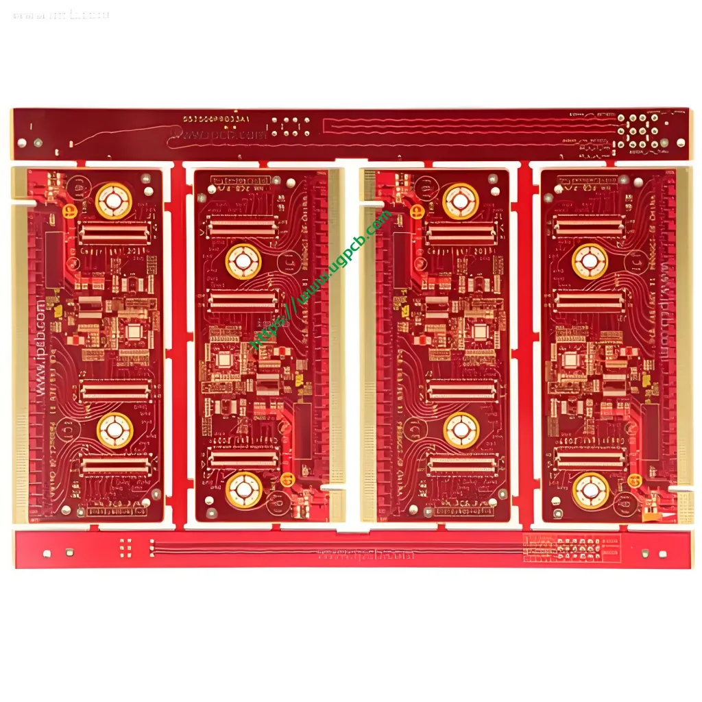
On a 回路基板 with a thickness of merely 1.2mm, the vivid red solder mask creates a striking contrast with the lustrous gold fingers. This is not merely an aesthetic choice but a critical design feature that ensures stable high-frequency signal transmission.
Gold fingers consist of numerous gold-plated conductive contact tabs. They are named for their finger-like arrangement and gold-plated surface. With the rapid advancement of 5G communication, high-end medical devices, および自動車エレクトロニクス, traditional connection methods can no longer meet the escalating demands for high-density interconnection and signal integrity.
UGPCB has developed the Red Solder Mask + Bonding Gold Finger PCB precisely for this market need. By integrating advanced Electroless Nickel Immersion Gold (同意する) surface finish and specialized wire bonding technology, it provides a stable and reliable micro-connection solution between chips and circuit boards.
01 Product Core Definition
The Red Solder Mask Bonding Gold Finger PCB is, 名前が示すように, a specialized printed circuit board that integrates three key technical features. It incorporates a red solder mask ink, bonding pad areas designed for wire bonding processes with an ENIG finish, and a special structural design that supports chip interconnection via bonding.
This product primarily utilizes KB-6160C FR-4 substrate, an epoxy glass cloth copper-clad laminate with UV blocking functionality. It is suitable for boards requiring bi-directional simultaneous photosensitive solder mask curing and optical automated inspection, offering performance comparable to KB-6150.
Physically, the product features a standard double-layer design with a finished board thickness tightly controlled at 1.2mm and a copper weight of 1 オンス (約. 35μm). This specification balances structural strength and electrical performance while meeting the general thickness requirements for most electronic devices. A minimum trace/space design of 4 ミル (0.1mm) ensures signal integrity in high-density routing scenarios.
02 Wire Bonding Technology Explained
Wire bonding is a method in chip production used to connect a chip’s internal circuits to the package leads or the gold-plated copper foil on the bonding board using gold or aluminum wires, prior to encapsulation.
Ultrasonic waves (typically 40-140KHz) from a generator are converted into high-frequency vibration by a transducer and transmitted to a bonding wedge through a horn. When the wedge contacts the wire and the bonding pad, pressure and vibration cause the metal surfaces to frictionally interact under controlled force. This process breaks down oxide layers, induces plastic deformation, and brings pure metal surfaces into intimate contact at an atomic distance, ultimately forming a strong mechanical bond.
This technology is primarily applied in scenarios involving ultra-small chips or bare die installation that cannot be mounted via standard SMT processes. Compared to traditional soldering, wire bonding provides finer interconnect capability, supporting smaller pitches and higher densities, making it particularly suitable for microelectronic devices with extreme integration requirements.
03 Advantages of ENIG Surface Finish
The product employs エレクトロレスニッケルイマージョンゴールド (同意する) as its surface finish, a choice based on multiple technical considerations. ENIG deposits nickel and gold only on the pads, resulting in stronger adhesion between the solder mask and the copper layer on the traces. This allows for engineering compensation without affecting spacing.
ENIG boards offer excellent surface flatness そして shelf life, comparable to electroplated gold boards. Compared to electroplating, ENIG produces a denser, more uniform crystalline structure with a purer golden color. This structure provides superior solderability and enhanced oxidation resistance.
のために high-frequency signal transmission, ENIG offers distinct advantages. Since the nickel-gold layer exists only on the pad areas, signal transmission via the skin effect primarily occurs within the copper layer. This avoids the potential negative impact on high-frequency signal quality that can occur with full-board gold plating. さらに, the ENIG process completely eliminates the “gold wire short circuit” issue possible with electroplated gold boards, thereby enhancing product reliability. The requirements for such finishes in bonding applications are detailed in standards like IPC-4556A.
04 Design Essentials and Specifications
Designing a PCB for bonding requires adherence to a series of special specifications to ensure the successful implementation of the wire bonding process.
Bonding pad surface finish is critical. The material and its structure must be compatible with the available bonding methods. The bonding surface must be clean, free from contaminants, fingerprints, or even microscopic pollutants. Bonding areas should be flat with uniform thickness, devoid of surface damage or irregularities. The surface metal should have hardness comparable to the bonding wire and must be bondable, which can be verified through bond pull tests.
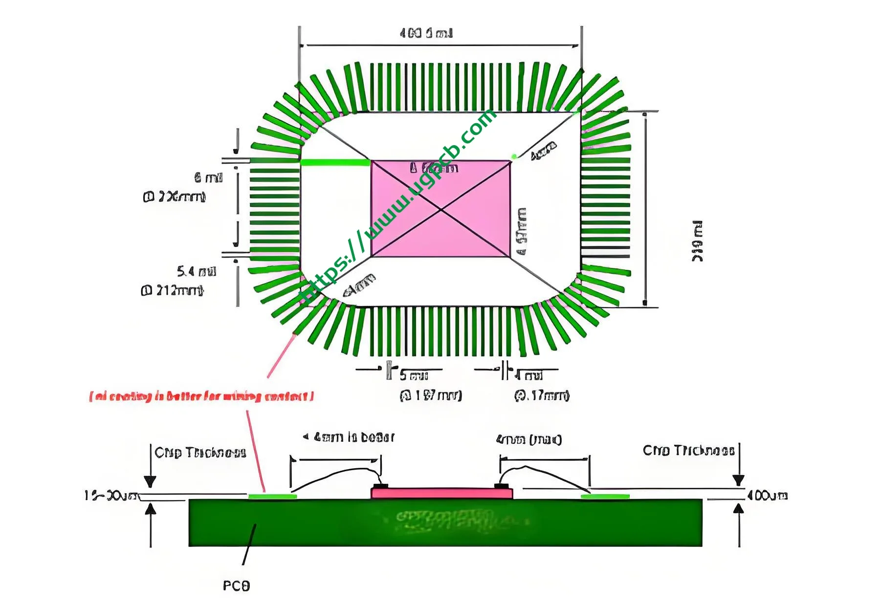
The shape and size of the bonding pads directly influence bonding quality. For aluminum wedge bonding, a more rectangular pad form is preferable, while gold ball bonding is better suited for square pads. From a hybrid circuit design perspective, designing bonding pads as large as possible is wise, as it provides greater flexibility for bond placement, chip positioning, and the repeatable alignment of fiducials to the bonding pads.
Spacing and layout also require special attention. A bonding pitch of 60µm is feasible when using 25µm wire diameter. しかし, loop height will be limited due to the need for dual-sided relief tools for fine-pitch aluminum wedge bonding. The minimum preferred straight-line distance between two bonds is 300µm, depending on the tooling and, to some extent, the loop shape.
These design considerations align with the foundational principles outlined in the IPC-2221C, the generic standard for printed board design.
05 Material Property Analysis
The KB-6160C substrate used in the product is a high-performance FR-4 epoxy glass cloth copper-clad laminate produced by Kingboard. This material features UV blocking functionality, making it particularly suitable for PCB production requiring bi-directional simultaneous photosensitive solder mask curing and optical automated inspection.
標準FR-4との比較, KB-6160C offers more stable dimensional control and thermal performance while maintaining excellent mechanical and electrical properties. This stability is crucial for the thermosonic bonding process involved in wire bonding.
の選択 red solder mask ink is not merely aesthetic but holds practical engineering value. Red PCBs offer excellent visibility and clearly define the contrast between traces, planes, and blank areas. Silkscreen printing appears very distinct on a red PCB background. The high contrast between white silkscreen and the red solder mask greatly facilitates subsequent assembly and inspection work.
06 Detailed Production Process
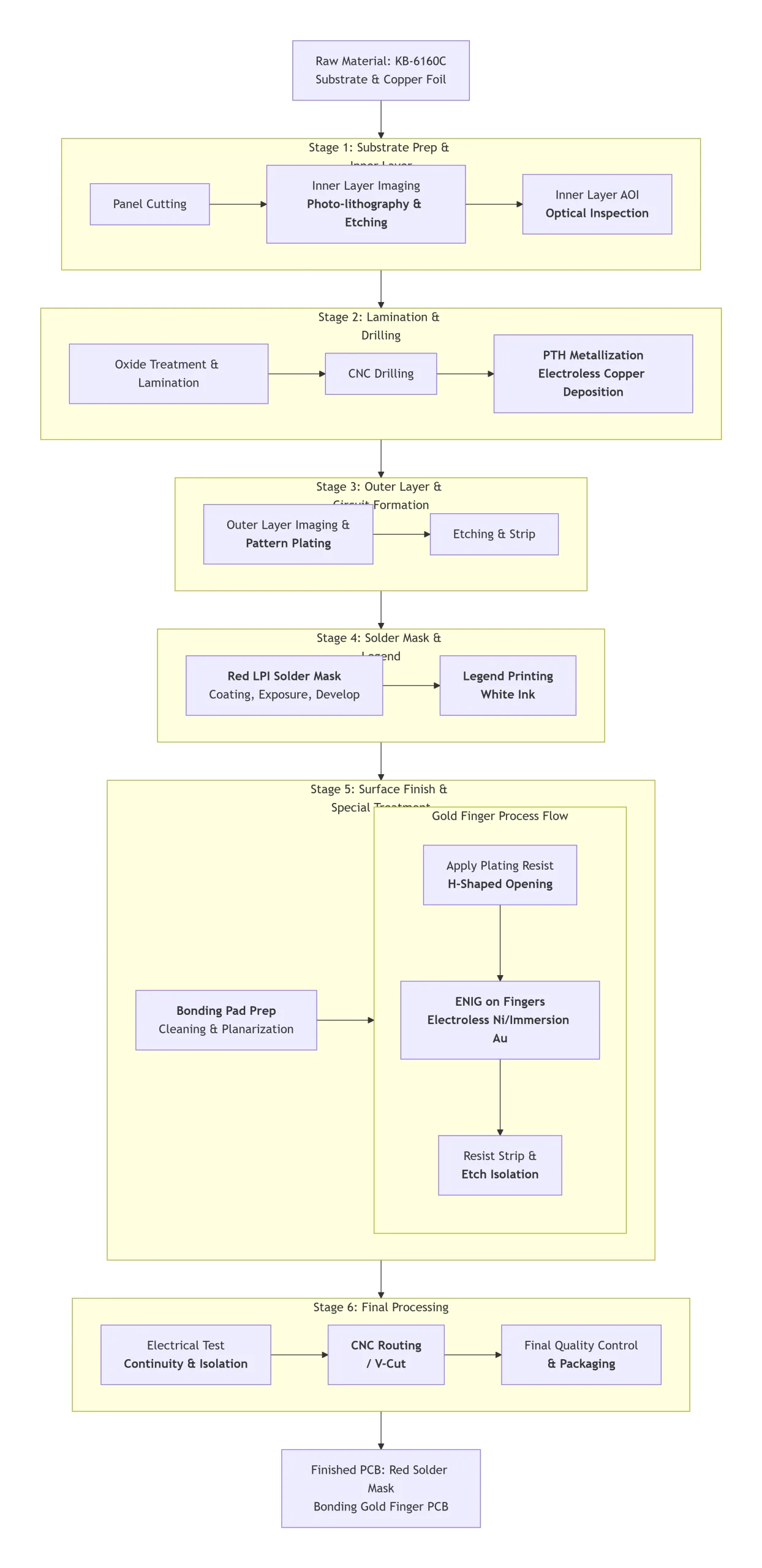
The manufacturing of Red Solder Mask Bonding Gold Finger PCBs integrates standard double-sided board processes with multiple special treatments. The main workflow is as follows:
-
Panelization and Inner Layer Processing: The KB-6160C substrate is cut to size per design requirements. Inner layer circuit patterning and etching follow. Bonding areas receive special treatment to ensure copper surface cleanliness and flatness.
-
Drilling and Metallization: High-precision drilling equipment creates via holes. Chemical copper plating then metallizes the holes to ensure reliable interlayer connection.
-
Circuit Pattern Transfer: The circuit pattern is transferred to the panel surface via photolithography, followed by pattern plating to increase copper thickness on the traces.
-
Solder Mask and Surface Finish: Red solder mask ink is applied and developed to open windows on pads. The ENIG process is then performed. ここ, the nickel layer acts as a barrier to prevent copper-gold interdiffusion, while the gold layer provides an excellent contact surface.
-
Special Treatment for Bonding Areas: The gold finger bonding zones undergo fine cleaning and planarization to meet the stringent surface quality requirements of the bonding process.
-
Silkscreen and Routing: White ink is used for silkscreen printing. ついに, the board outline is completed using CNC routing or die punching.
07 Summary of Performance Characteristics
The Red Solder Mask Bonding Gold Finger PCB synthesizes multiple technological advantages. Its main performance features include:
-
優れた高周波性能: The ENIG-treated gold finger area provides a low-resistance, stable contact interface. Combined with the 4mil fine-line design, it ensures high-frequency signal integrity.
-
Superior Bonding Compatibility: The specially optimized bonding pad surface treatment ensures a high success rate and strong connection strength for both gold and aluminum wire bonding.
-
Long-Term Reliability: The ENIG layer offers strong oxidation resistance. The nickel barrier layer effectively prevents copper-gold diffusion, guaranteeing contact stability over long-term use.
-
High-Density Design Capability: Supports a 4mil minimum trace/space, meeting the high-density interconnection needs of modern electronic devices.
-
Precise Thickness Control: A 1.2mm finished thickness with strict tolerance control ensures compatibility and stable insertion/removal in various connectors.
08 Application Scenario Analysis
This professional PCB product primarily targets applications with stringent demands for connection reliability, 信号の完全性, and space utilization:
-
ハイエンド通信機器: Chip interconnects in 5G base stations, 高速ルーター, and optical communication modules require stable and reliable high-frequency signal transmission channels.
-
Medical Electronic Devices: Micro-sensor interfaces in portable medical monitors and implantable medical devices have extreme requirements for connection reliability and size.
-
Automotive Electronic Systems: High-density chip interconnects in Advanced Driver-Assistance Systems (アダス) and infotainment system controllers. Standards like IPC J-STD-001JA/IPC-A-610JA address the rigorous requirements for such automotive applications.
-
産業制御機器: Signal acquisition and processing modules in industrial automation controllers and precision measurement instruments.
-
High-End Consumer Electronics: Mainboard-to-subboard connection interfaces in ultra-thin laptops and premium smartphones.
The common thread across these fields is the need for miniaturized, highly reliable chip-level interconnection solutions, where traditional connectors or 標準のPCB can no longer meet the technical requirements.

09 Choosing a Professional Manufacturer
Choosing UGPCB as your supplier for Red Solder Mask Bonding Gold Finger PCBs grants access to comprehensive professional services from design support to volume production.
With deep expertise in wire bonding processes, we provide targeted design optimization advice to help clients avoid common bonding failure issues. Our advanced production equipment ensures consistency in 4mil fine-line patterning and ENIG thickness. A stringent quality control system covers the entire process from raw material inspection to final testing.
Specifically for bonding PCBs, UGPCB has established specialized procedures for bonding area cleanliness control そして surface flatness inspection standards, ensuring every circuit board meets the exacting requirements of the bonding process. Our manufacturing practices are informed by globally accepted IPC標準, which help ensure quality, 信頼性, and consistency throughout the electronics manufacturing process.
As electronic products evolve to be shorter, 小さい, lighter, and thinner, the PCB industry faces both opportunities and new challenges. As a professional PCB manufacturer, UGPCB is committed to providing high-performance, high-reliability circuit interconnection solutions through technological innovation and process optimization, helping our clients’ products excel in a competitive market.
Beneath the red solder mask of this circuit board, the miniature gold fingers shimmer with a uniform luster under professional equipment. They are the bridges connecting chips to the external world.
As test probes gently contact the gold finger surface, electrical parameters display steadily on screens, and high-frequency signals flow smoothly along the precisely designed traces. After rigorous testing, these circuit boards will ultimately be installed at the heart of high-performance devices, silently ensuring the accuracy and stability of every signal exchange.


