
Rogers RO4725JXR PCB ラミネート: The Ultimate Solution for High-Performance RF & Antenna Applications
When your design pushes high-frequency limits, your choice of PCBラミネート 重要です.
In the rapidly evolving fields of 5G communications, 高度なドライバーアシスタンスシステム (アダス), およびIoTデバイス, engineers are constantly pushing the boundaries of high-frequency PCB design. Balancing signal loss, 熱安定性, and cost-effectiveness remains a persistent challenge in designing RF circuit boards and antenna feed networks. UGPCB’s Rogers RO4725JXR series is engineered to resolve this core conflict—seamlessly integrating superior RF performance, 優れた信頼性, and competitive cost. It is the ideal foundation for building next-generation wireless systems.
Product Deep Dive: Redefining Performance Standards for Antenna-Grade PCBs
製品の定義 & 科学的分類
The Rogers RO4725JXR™ PCB laminate is a ceramic-filled PTFE (ポリテトラフルオロエチレン) composite-based high-frequency material, scientifically classified as an antenna-grade, low-loss microwave substrate. It is not a standard printed circuit board material but an engineered substrate designed for demanding RF and microwave applications. Its performance sits between standard FR-4 and pure PTFE laminates, achieving the optimal balance between performance and manufacturability.
Core Performance Parameters: The Engineering Advantages Behind the Data
| Performance Parameter | 仕様 | Implication for Your Design |
|---|---|---|
| 誘電率 (DK) | 2.55 ± 0.05 | Excellent stability ensures consistent impedance from baseband to mmWave frequencies. It is fundamental for designing precise microstrip and stripline PCBs, directly determining signal integrity and antenna radiation efficiency. |
| 損失係数 (Df) | 0.0022 @ 2.5 GHz | Industry-leading low-loss characteristic. A Df of just 0.0022 で 2.5 GHz means minimal signal energy loss within the substrate in 5G Sub-6GHz bands, significantly improving system Signal-to-Noise Ratio (SNR) and overall efficiency. |
| Z軸CTE | < 30 ppm/°C | Closely matches the CTE of copper, virtually eliminating the risk of plated through-hole (PTH) failure due to thermal cycling. This is crucial for high-reliability PCBs subjected to extreme temperature swings or multiple reflow cycles. |
| Glass Transition Temp (TG) | >280℃ (536°F) | Exceptionally high thermal endurance ensures mechanical and electrical properties do not degrade during lead-free soldering processes. Suitable for demanding applications like automotive electronics. |
| 銅箔 | 控えめ (Low Roughness) Foil | Effectively reduces conductor loss from the “表皮効果” 高周波で. A key factor for ensuring final performance in mmWave circuit board designs above 10GHz. |
| Process Compatibility | Compatible with Standard FR-4 Processes | Can be processed on standard PCB production lines. Supports hybrid construction (mixed lamination) with FR-4, greatly reducing complexity and cost from prototype to volume production. |
| 環境コンプライアンス | ROHS準拠 | Meets global environmental regulations for unrestricted market access. |
設計上の重要な考慮事項
-
インピーダンス制御: Utilize its stable, known Dk value (2.55) combined with UGPCB’s advanced calculation tools to achieve precise impedance control within ±5%.
-
Thermal Management Design: Excellent Z-axis CTE allows for more confident use of multi-stage blind and buried via structures in multilayer 高密度相互接続 (HDI) PCBデザイン, without compromising long-term reliability.
-
Loss Budget: The extremely low Df value enables designers to allocate a more generous loss margin in the link budget or to design longer, more complex low-loss feed networks.
材料構成, 構造 & Core Features
-
材料: A ceramic-powder-filled PTFE composite substrate clad with ultra-low-profile electro-deposited copper foil. This unique formulation retains PTFE’s excellent dielectric properties while the ceramic filler enhances mechanical strength, 熱伝導率, and significantly reduces material cost.
-
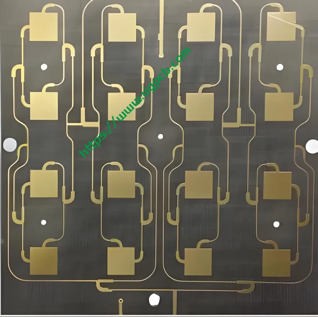
構造: Supplied as standard Copper Clad Laminate (CCL). Available in various standard thicknesses (例えば。, 0.254mm, 0.508mm, 0.762mm) and copper weights (1オンス, 0.5オンス) to manufacture single-sided, 両面, or multilayer high-frequency hybrid dielectric PCBs.
-
コアの利点:
-
Optimal Performance-Cost Balance: Delivers RF performance close to pure PTFE laminates with better cost-efficiency and easier processing. The ideal choice for projects demanding high performance and cost control.
-
Exceptional Long-Term Reliability: The combination of very low Z-axis CTE (<30 ppm/°C) and ultra-high Tg (>280℃) ensures extended lifespan and stable operation in harsh environments like outdoor base stations and automotive systems.
-
End-to-End Low-Loss Solution: 低誘電損失 (Df) and low-profile copper foil work synergistically to minimize signal attenuation from both the dielectric and conductor, making it the premier choice for low-loss PCB fabrication.
-
Seamless Integration into Existing Supply Chains: Fully compatible with standard epoxy/glass (FR-4) PCB fabrication processes—including drilling, desmear, メッキ, imaging, and soldermask application. Requires no special equipment or processes, shortening the learning curve and improving production yield.
-
From Laminate to Finished Product: Our Refined Production Process
UGPCBへ, we employ an optimized, proprietary process flow for Rogers RO4725 series laminates to ensure their innate superior performance is fully realized:
材料の準備 & Inner Layer Fabrication → AOI Inspection → Lamination & Pressing (supports FR-4 hybrid) → Laser/Mechanical Drilling → Hole Metallization & Plating → Outer Layer Imaging → High-Performance Soldermask Coating → Surface Finish (同意する, Immersion Silver recommended) → 100% Flying Probe/Fixture Electrical Testing → Final Visual & Dimensional Inspection. We place particular emphasis on three critical quality control points: impedance control consistency, hole wall quality, and layer-to-layer registration accuracy.
典型的なアプリケーション: Enabling Cutting-Edge Technology
-
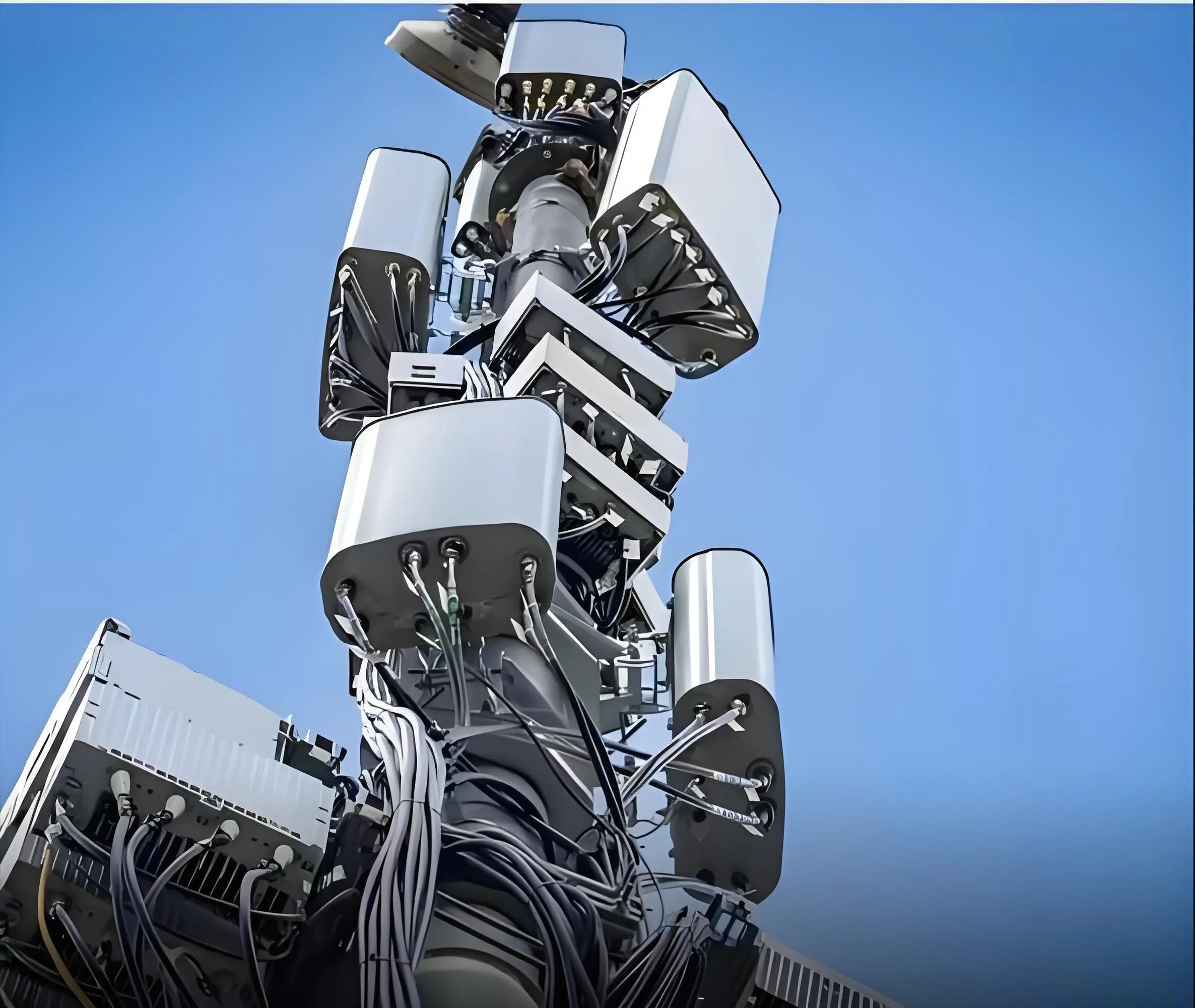
Cellular Communication Infrastructure: The classic application for 4G/LTE and 5G Sub-6GHz macro and micro base station antenna radiating elements, feed networks, and filters.
-
RF Identification Systems: High-performance UHF RFID reader antennas requiring low loss and stable radiation pattern performance from the substrate.
-
カーエレクトロニクス & Radar: Printed Circuit Boards for 77GHz automotive radar sensors (例えば。, corner radar, forward-facing radar), where stable Dk is crucial for beamforming accuracy.
-
衛星通信 & Broadcast: Low-Noise Amplifier (LNA) and down-converter circuits in VSAT terminals and LNBs.
-
General High-Performance RF Modules: Point-to-point microwave backhaul, test instrumentation, medical imaging equipment, and any field requiring high-performance RF PCBs.
UGPCBを選択します: Your Trusted Partner in High-Frequency PCBs
We provide not only genuine Rogers RO4725JXR laminates but also end-to-end technical solutions:
-
Technical & Supply Chain Assurance: As an authorized partner, we guarantee reliable material sourcing with performance matching the datasheet.
-
In-Depth PCB Design Support: Free stack-up design, impedance calculation, and Design for Manufacturability (DFM) analysis to minimize your design risks.
-
Proven Hybrid Dielectric Board Expertise: Extensive experience in manufacturing high-frequency hybrid PCBs ensures perfect bonding between RO4725 and FR-4 for robust, reliable structures.
-
迅速な応答 & Flexible Delivery: から PCBプロトタイピング to quick-turn low/medium-volume production, we offer highly competitive lead times.


