

Introduction to Wireless Charging PCB
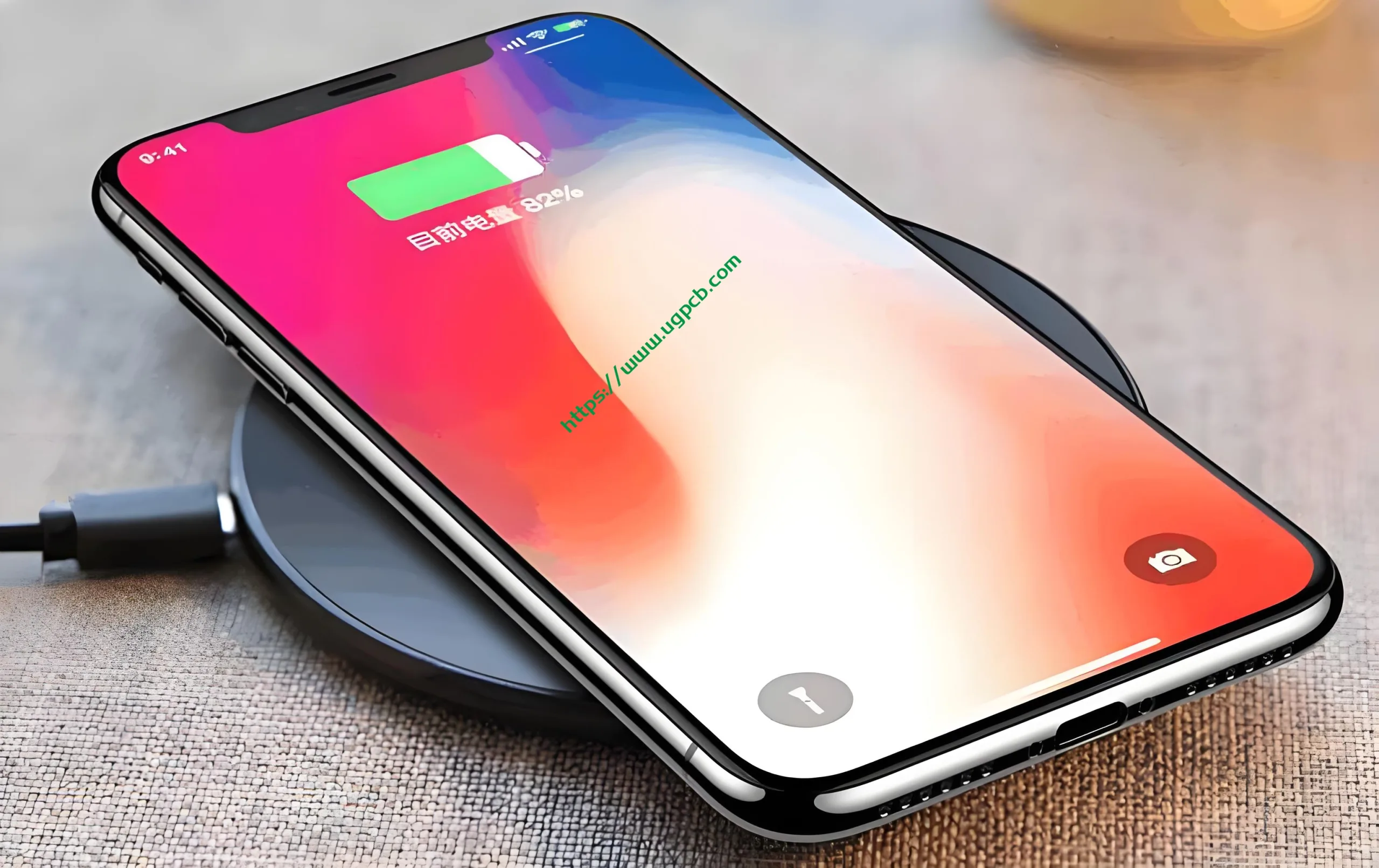
A Wireless Charging PCB, also known as an inductive charging 回路基板, is a specialized printed circuit board designed for wireless power transfer. It enables devices such as smartphones, 錠剤, and other electronic gadgets to be charged without the need for physical connectors.
作業原則
Wireless charging technology operates on the principle of electromagnetic induction. The transmitter coil generates an alternating electromagnetic field that induces a current in the receiver coil, thus transferring energy from the charger to the device.
アプリケーション
Wireless Charging PCBs are widely used in consumer electronics for charging devices like mobile phones, スマートウォッチ, earbuds, and even electric toothbrushes. They offer convenience, ease of use, and reduced wear and tear on charging ports.
Types of Wireless Charging PCBs
There are two main types of wireless charging technologies:
- Qi Standard: The most common and widely adopted wireless charging standard.
- PMA (Power Matters Alliance): Another popular standard, often found in older devices.
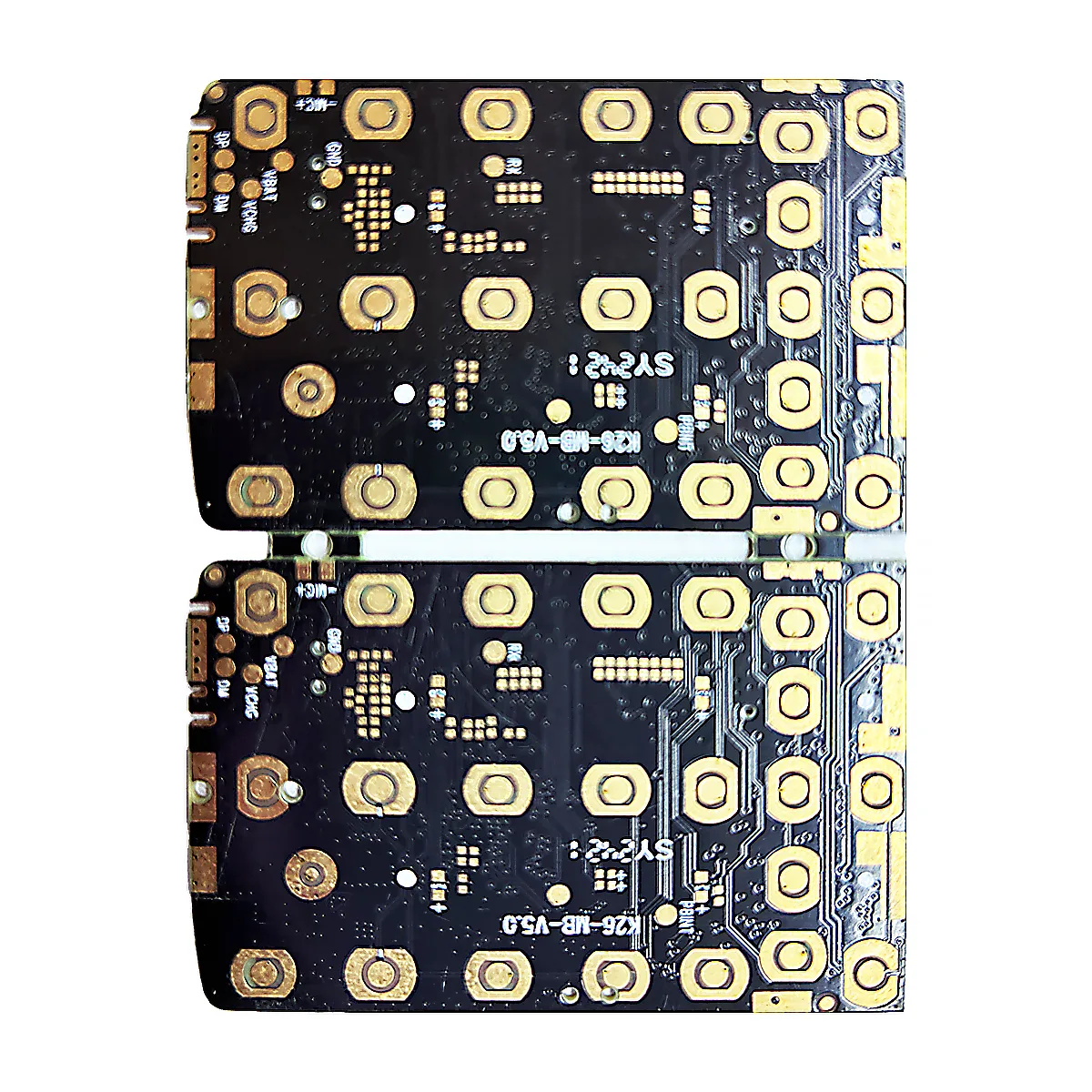
材料と建設
- 材料: S1000-2, 高品質のエポキシ素材.
- レイヤー: 6 レイヤー, 堅牢性とより優れた信号整合性を提供します.
- 色: 緑または白からお選びいただけます.
- 仕上がり厚さ: 1.2mm, スリムでありながら耐久性を確保.
- 銅の厚さ: 2オズ, 良好な導電性を提供します.
- 表面処理: Immersion gold with a thickness of at least 2U”, 耐食性とはんだ付け性の向上.
- 穴の銅の厚さ: 351つ, ensuring strong connections.
- 最小開口: 0.4mm, allowing for fine detail work.
性能特性
Wireless Charging PCBs are designed to efficiently transfer power with minimal loss. They support fast charging capabilities and are built to withstand repeated usage over time. イマージョンゴールド仕上げにより、長期にわたるパフォーマンスと信頼性が保証されます。.
構造的特徴
The structure of a Wireless Charging PCB includes multiple layers of copper traces sandwiched between layers of substrate material. この多層設計は、熱放散の管理と電気的性能の向上に役立ちます。. The プリント基板 is coated with a protective layer to prevent damage and ensure longevity.
製造工程
The production of a Wireless Charging PCB involves several steps:
- デザイン: 専用ソフトを使用して回路レイアウトを作成.
- エッチング: 余分な銅を除去して目的のパターンを形成します.
- ラミネート加工: 複数のレイヤーを結合する.
- メッキ: 金属の薄い層を追加して接続性を向上させる.
- 検査: PCB が品質基準を満たしていることを確認する.
- 組み立て: コンポーネントを PCB に実装する.
- テスト: 機能や性能の検証.

ユースケース
Wireless Charging PCBs are used in various applications including:
- 家電: 携帯電話, 錠剤, スマートウォッチ.
- 自動車: In-car charging systems for smartphones.
- 医療機器: 携帯型医療機器.
- ウェアラブル: Fitness trackers, smart rings.
結論は, Wireless Charging PCBs represent a significant advancement in charging technology, offering convenience, 効率, そして耐久性. さまざまな業界で広く採用されていることから、現代の電子機器におけるその多用途性と重要性が浮き彫りになっています。.


