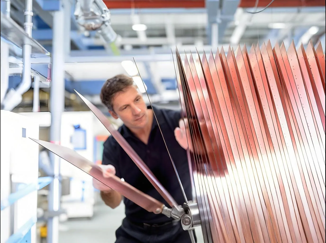
F4BMX-1/2 Teflon PCBの概要
F4BMX-1/2 is a high-performance laminate crafted by layering imported varnished glass cloth with Teflon resin and Polytrtrafluoroethylene film. この製品は、科学的製剤と厳しい技術プロセスに準拠しています, offering superior electrical performance compared to the F4B series. It features a broader range of dielectric constants, 誘電正接が低い, 抵抗の増加, より安定したパフォーマンス. The use of imported woven glass fabric ensures consistency in the properties of the laminate.
F4BMX-1/2 Technical Specifications
外観
Meets the specification requirements for microwave PCB laminates according to national and military standards.
種類
- F4BMX217
- F4BMX220
- F4BMX245
- F4BMX255
- F4BMX265
- F4BMX275
- F4BMX285
- F4BMX294
- F4BMX300
誘電率
- F4BMX217: 2.17
- F4BMX220: 2.20
- F4BMX245: 2.45
- F4BMX255: 2.55
- F4BMX265: 2.65
- F4BMX275: 2.75
- F4BMX285: 2.85
- F4BMX294: 2.94
- F4BMX300: 3.0
寸法 (mm)
- Standard dimensions available: 300250, 380350, 440550, 500500, 460610, 600500, 840840, 8401200, 15001000, 18001000
- Customized dimensions are also available.
厚さと寛容 (mm)
| ラミネートの厚さ | 許容範囲 |
|---|---|
| 0.25 | ±0.025 |
| 0.5 | ±0.05 |
| 0.8 | ±0.05 |
| 1.0 | ±0.05 |
| 1.5 | ±0.075 |
| 2.0 | ±0.09 |
| 3.0 | ±0.1 |
| 4.0 | ±0.1 |
| 5.0 | ±0.1 |
| 6.0 | ±0.12 |
| 8.0 | ±0.15 |
| 10.0 | ±0.18 |
| 12.0 | ±0.2 |
注記: ラミネートの厚さには、銅の厚さが含まれます. カスタマイズされたラミネートは、特別な寸法で利用できます.
機械的強度
| 厚さ(mm) | 最大ワープ | Original Board | 片側 | 二重側 |
|---|---|---|---|---|
| 0.25~0.5 | 0.030 | 0.050 | 0.025 | 0.020 |
| 0.8~1.0 | 0.025 | 0.030 | 0.020 | 0.020 |
| 1.5~2.0 | 0.020 | 0.025 | 0.015 | 0.015 |
| 3.0~5.0 | 0.015 | 0.020 | 0.010 | 0.010 |
切断/パンチング強度:
- For thickness <1mm, 切断後のバリはありません; 2つのパンチングホール間の最小スペースは0.55mmです, 剥離はありません.
- For thickness >1mm, 切断後のバリはありません; 2つのパンチングホール間の最小スペースは1.10mmです, 剥離はありません.
皮の強度 (1オンスの銅用):
- 通常の状態: ≥18n/cm; バブルまたは剥離皮の強度はありません: ≥15n/cm (一定の湿度と温度で, and kept in molten solder at 260 学位摂氏±2度摂氏 20 秒).
化学物質
PCBの化学エッチング方法は、ラミネートの誘電特性を変更せずに使用できます. 穴を介したメッキには、ナトリウム治療または血漿治療が必要です. Hot Air Level temperature must not exceed 253 degrees Celsius and cannot be repeated.
電気物質
| 名前 | テスト条件 | ユニット | 価値 |
|---|---|---|---|
| 密度 | 通常の状態 | g/cm³ | 2.1~2.35 |
| 水分吸収 | 20±2°Cで蒸留水に浸します 24 時間 | % | ≤0.08 |
| 動作温度 | 高温チャンバー | 学位摂氏 | -50°C+260°C |
| 熱伝導率 | w/m/k | 0.3~0.5 | |
| CTE | Typical (εr :2.1〜2.3) | ppm/°C | x: 24(x), y: 34(y), z: 235(z) |
| CTE | Typical (εr :2.3〜2.9) | ppm/°C | x: 16(x), y: 20(y), z: 168(z) |
| CTE | Typical (εr :2.9~3.38) | ppm/°C | x: 12(x), y: 15(y), z: 92(z) |
| 収縮係数 | 2 沸騰したお湯の時間 | % | < 0.0002 |
| 表面抵抗率 | 直流, 500V, 通常の状態 | MΩ | ≥2*10^5 |
| Under constant humidity and temperature | ≥8*10^4 | ||
| 体積抵抗率 | 通常の状態 | MΩ・cm | ≥8*10^6 |
| Under constant humidity and temperature | ≥2*10^5 | ||
| 表面誘電強度 | 通常の状態 | D = 1mm(KV/mm) | ≥1.2 |
| Under constant humidity and temperature | ≥1.1 | ||
| 誘電率 | 10GHz, εr | (±2%) | 以下の表を参照してください |
| 損失係数 | 10GHz tgδ | 以下の表を参照してください |
Dielectric Constant and Dissipation Factor at 10GHz
| タイプ | 誘電率 (εr) | 損失係数 (tgside) |
|---|---|---|
| F4BMX217 | 2.17 | – |
| F4BMX220 | 2.20 | – |
| F4BMX245 | 2.45 | – |
| F4BMX255 | 2.55 | – |
| F4BMX265 | 2.65 | – |
| F4BMX275 | 2.75 | – |
| F4BMX285 | 2.85 | – |
| F4BMX294 | 2.94 | – |
| F4BMX300 | 3.0 | – |
UGPCB Products and Services
UGPCB offers a variety of products including Radio/Microwave/High Frequency hybrid circuits, single layer to multilayer AnyLayerHDI, BGA, IC Heavy Copper Board, and custom solutions such as Rigid-Flex, HDI, Blind Buried Slotted Blind Back Drilled, and IC Carrier boards. Our services include PCB manufacturing, 電気めっき, もっと. For any inquiries, please contact us through our website www.ugpcb.com or email us at sales@ugpcb.com.
