ITEQ IT-158 PCB 基板材料
キーパフォーマンスパラメーター & 技術的な利点
ITEQ IT-158ラミネートは、最高の選択肢として現れます ハイエンドPCB 例外的な技術仕様を通じて製造:
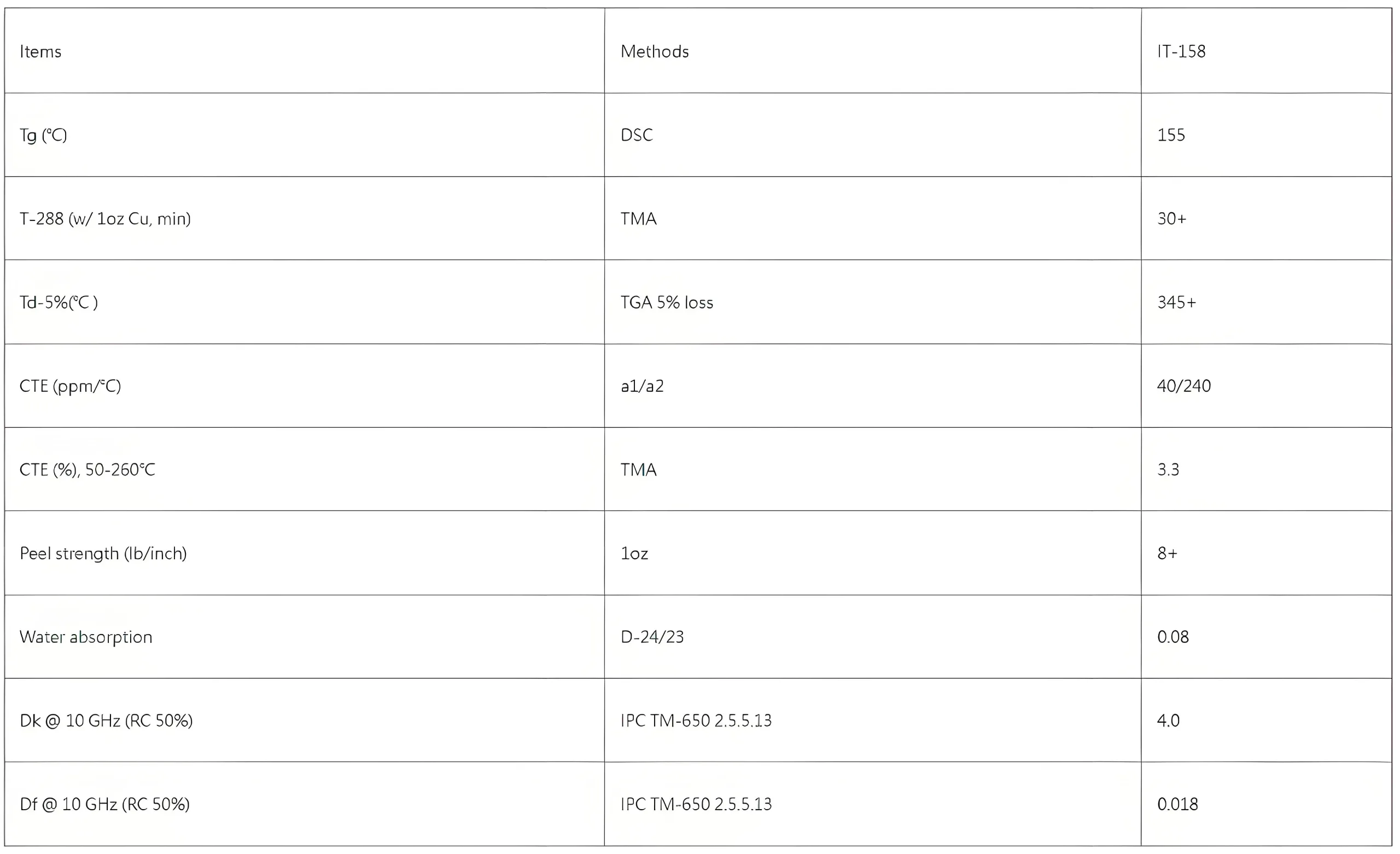
熱信頼性
-
TG: 155℃ (鉛フリーのはんだ中に構造の安定性を保証します)
-
T-288: >30 288°Cで秒 (優れた熱衝撃耐性)
-
TD-5%: 345℃ (極端な条件での剥離を防ぎます)
機械的安定性
-
Z軸CTE: 40ppm/°C (3.3% 50-260°Cからの拡張)
-
はく離強度: ≥8lb/インチ (銅に覆われた結合の完全性)
-
吸水性: 0.08% (電気の安定性を維持します 85% RH環境)
高周波信号伝送特性
10GHzでの誘電性パフォーマンス
-
DK: 4.0 ±0.05
-
Df: 0.018
*(0.15dB/インチの挿入損失削減を備えた5G/MMWAVEアプリケーションに最適です)*
典型的なアプリケーションシナリオ
5G通信インフラストラクチャ
-
ベースステーションアンテナ
-
光トランシーバー
カーエレクトロニクス
-
ADASレーダーシステム (AEC-Q200互換性)
-
ECU制御モジュール
産業用自動化
-
サーボドライブ (10,000105°CのHR MTBF)
-
パワーインバーター
家電
-
スマートフォンRFモジュール
-
ラップトップマザーボードHDIデザイン
PCB材料選択ワークフロー
段階 1: 要件分析
-
動作温度範囲: Tmax +20°Cマージン
-
信号周波数のしきい値: ≥1GHzクリティカル
-
環境評価: IP67コンプライアンス
段階 2: 比較評価
| パラメーター | ITEQ IT-158 | 競争相手a | 競合他社b |
|---|---|---|---|
| TG (℃) | 155 | 140 | 130 |
| DF @10GHz | 0.018 | 0.025 | 0.032 |
| UL認定 | 94V-0 | 94HB | 94V-1 |
段階 3: 信頼性の検証
-
PCTテスト: 121°C/100%RH/2ATM×96HR
-
熱応力: 3×はんだディップ @288°C
-
カフェ抵抗: IPC-TM-650 2.6.25 準拠
設計最適化戦略
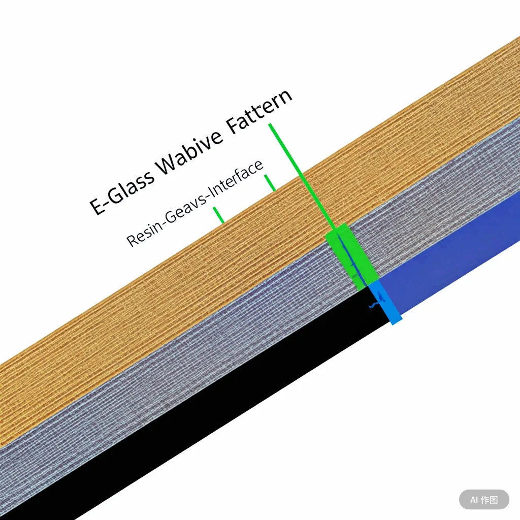
スタックアップ構成
-
ハイブリッド誘電構造 (≤5%の厚さ耐性)
-
熱管理のための埋葬VIA
インピーダンス制御
-
マイクロストリップライントレランス: ±10%
-
微分ペア間隔: 3×誘電体の高さ
製造工程
-
掘削: 0.15mm以下のスタブでバックドリル
-
表面仕上げ: Enepigが望ましい (で:3-5μm, au:0.05-0.1μm)
ITEQ IT-158 PCB 基板パラメータ表

主題の実際の有益で素晴らしい解剖学的構造, これでユーザーフレンドリーになりました (:.