
UGPCB: 고급 HDI PCB 기술을 통한 선구적인 고밀도 인터커넥트 혁신
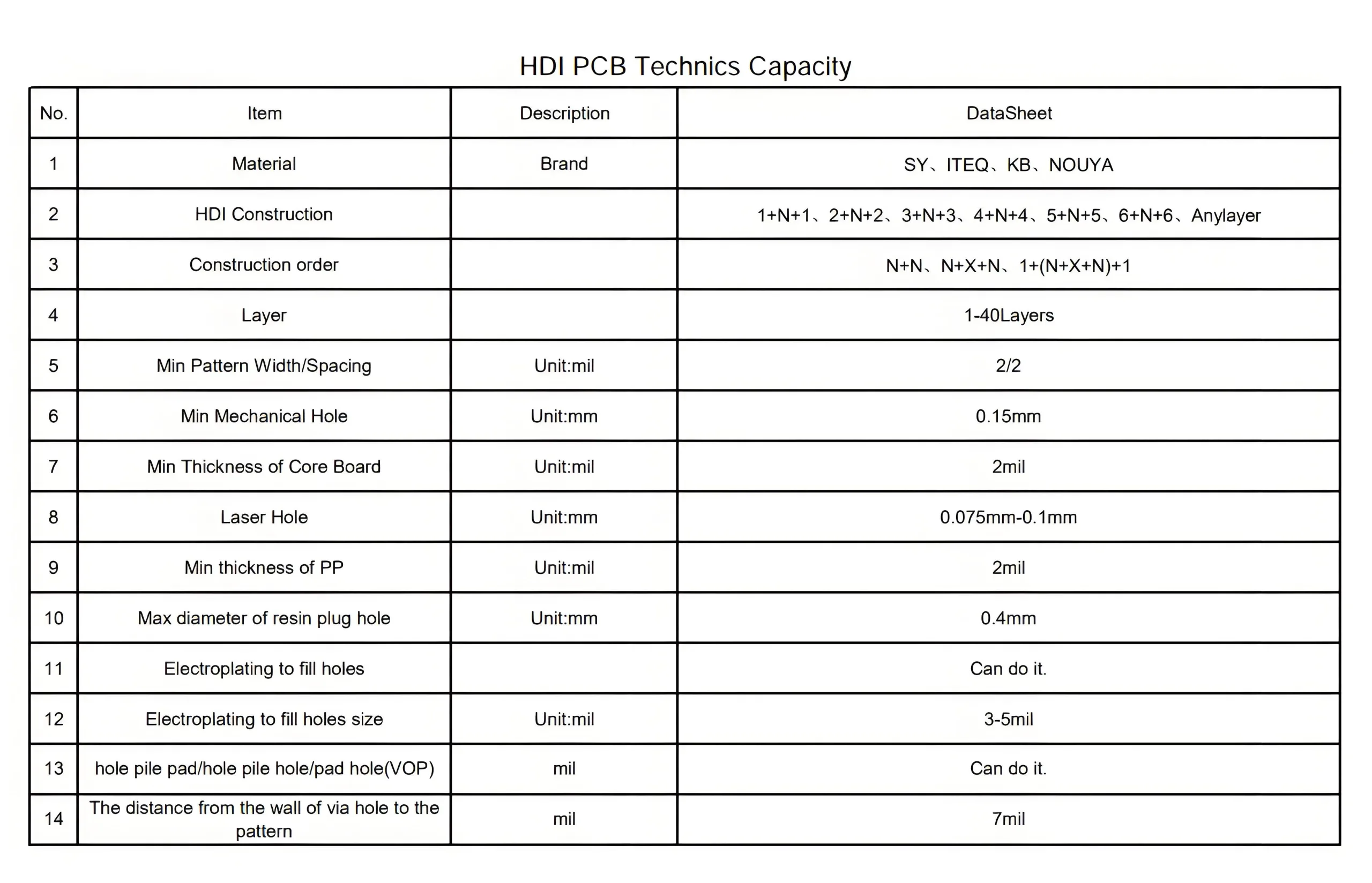
업계 최고의 HDI PCB 제조 역량
UGPCB 선두에 서 있다 HDI (고밀도 상호 연결) PCB 기술, 전자기기가 전례 없는 두께와 기능성을 요구하는 시대의 발전을 주도. 전문적으로 4-40 두께가 0.4mm ~ 6.0mm인 레이어 다층 보드, 가전제품부터 프리미엄 통신장비까지 다양한 요구에 부응합니다..
당사의 최첨단 Any-layer HDI 기술은 전체에 걸쳐 원활한 상호 연결을 가능하게 합니다. 10 PCB 레이어, 고성능 컴퓨팅 및 통신 장치를 위한 강력한 연결 솔루션 제공. 이러한 역량을 통해 당사는 차세대 전자 애플리케이션을 위한 신뢰할 수 있는 파트너로 자리매김했습니다..
공정기술: 정밀도와 신뢰성의 만남
고급 장비 & 혁신
UGPCB는 최첨단 장비 및 프로세스 혁신을 통해 HDI PCB 제조 분야에서 업계 벤치마크를 설정합니다.:
- 레이저 드릴링: 0.075mm의 작은 마이크로비아 가공 실현 (3밀) 업계 표준을 뛰어넘는 정밀도로
- 마이크로 비아 기술: 다음 레이어 비아를 통한 숨겨진 상호 연결로 팬인/팬아웃 라우팅 제거, 회로 밀도를 대폭 향상
- 임피던스 제어: 유지하다 +/-7% 5G 및 고성능 컴퓨팅 애플리케이션에서 우수한 신호 무결성을 위한 임피던스 허용 오차

종합적인 제조 공정
우리의 HDI 생산 워크플로우는:
- 레이저 드릴링: CO₂ 레이저 시스템 일관된 홀 품질과 청결도 보장
- 도금공정: 12-18μm 구리 두께로 전기적 신뢰성 보장
- 패턴 전송: 초고밀도 라우팅을 위해 1.5/1.5mil의 최소 라인 폭/간격 지원
- 라미네이션 기술: ±200μm 이내의 레이어 정렬 정확도로 구조적 안정성 보장
우리는 고성능을 활용합니다 PCB 기판 높은 Tg FR-4 포함 (140/150/170℃) 고온 환경에서도 안정적인 성능을 보장하는 폴리이미드 소재.
품질 보증 & 테스트 시스템
다층 검사 프로토콜
UGPCB는 엄격한 품질관리를 통해:
- AOI (자동 광학 검사)
- 플라잉 프로브 테스트
- 엑스레이 검사
마이크로비아 신뢰성
당사 마이크로비아 기술의 고유한 신뢰성은 다음과 같습니다.:
- 더 얇은 구조 1:1 종횡비
- 기존 스루홀에 비해 신호 전송 안정성이 뛰어남
- 까다로운 응용 분야를 위한 향상된 장기 내구성
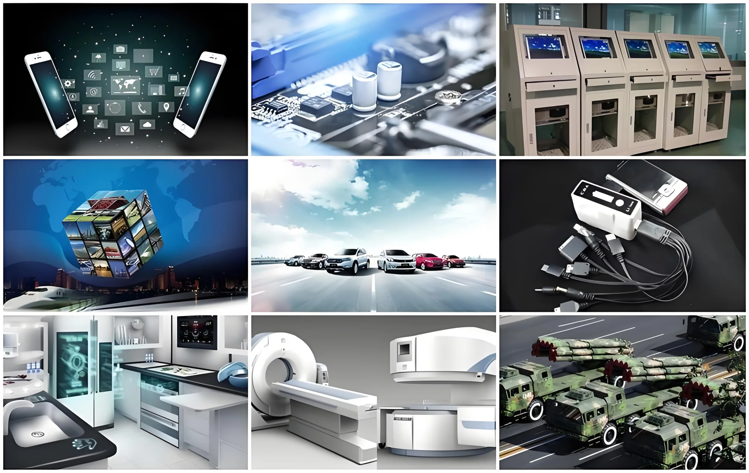
응용: 최첨단 기술 강화
UGPCB의 HDI PCB는 여러 부문에 걸쳐 첨단 기술 애플리케이션을 지원합니다.:
- 5지커뮤니케이션: 고주파 PCB 5G 기지국 및 RF 모듈용
- 자동차 전자: 내비게이션 및 엔터테인먼트 시스템을 위한 안정적인 신호 전송
- 의료 기기: 환자 모니터 및 수술 기구에 대한 정밀 데이터 수집
- 산업 제어: PLC 및 센서 네트워크를 위한 효율적인 데이터 교환

기술적 이점: UGPCB를 선택하는 이유는 무엇입니까??
우수한 성능 기능
- 공간 효율: 마이크로비아/블라인드 비아 설계로 PCB 설치 공간을 최대로 줄입니다. 30%
- 신호 무결성: Low-DK 소재는 고속 전송을 위한 신호 지연 및 누화를 최소화합니다.
- 디자인 유연성: 컴팩트한 공간에서 복잡한 회로 구현 가능
- 열 관리: 전용 열 레이어는 고전력 애플리케이션의 열 방출을 향상시킵니다.
아르 자형&D 방향 & 미래의 전망
차세대 기술 투자
UGPCB는 HDI PCB를 적극적으로 개발합니다.:
- 더 높은 밀도와 더 미세한 라인
- 낮은 신호 손실 특성
- 레이저 드릴링의 발전
- 나노물질 통합
- 스마트 제조 시스템
우리의 R&D 팀은 5G에 대한 고객 로드맵을 지원하기 위해 고급 마이크로비아 기술과 재료 혁신에 중점을 두고 있습니다., 일체 포함, 그리고 IoT 기기.
결론: 신뢰할 수 있는 HDI PCB 파트너
업계 리더십
HDI PCB 기술 리더로서, UGPCB가 제공하는:
- 고급 프로세스 기능
- 엄격한 품질 관리
- 지속적인 기술 혁신
종합적인 솔루션
스마트폰부터 자동차 시스템까지, 토털 고밀도 인터커넥트 솔루션을 제공합니다.. UGPCB를 선택한다는 것은 선택을 의미합니다.:
- 우수한 성능
- 믿을 수 있는 품질
- 기술적 선견지명
지금 UGPCB에 문의하세요 HDI PCB 기술이 어떻게 차세대 제품에 힘을 실어줄 수 있는지 알아보세요..