

eMMC PCB 패키지 기판 제품 개요
오늘날의 데이터 중심 세계에서, 임베디드 스토리지의 성능과 신뢰성은 매우 중요합니다. EMMC (내장형 멀티미디어 카드) 스마트폰의 핵심 저장 장치 역할, 정제, IoT 장치, 및 기타 가전제품. UGPCB, 심층적인 전문 지식을 활용하여 고밀도 상호 연결 (HDI) PCB 제조, 전문적인 제안을 제공합니다 eMMC 패키지 기판 PCB. HL832NS 소재를 4겹으로 설계, 초박형 구성, 이 기판은 고속을 위한 필수 플랫폼입니다., 메모리 컨트롤러 간의 안정적인 전기적 상호 연결, NAND 플래시가 죽다, 그리고 메인보드. 차세대 컴팩트 개발을 위한 최적의 솔루션입니다., 대용량 저장 모듈.
eMMC 패키지 기판 PCB란 무엇입니까??
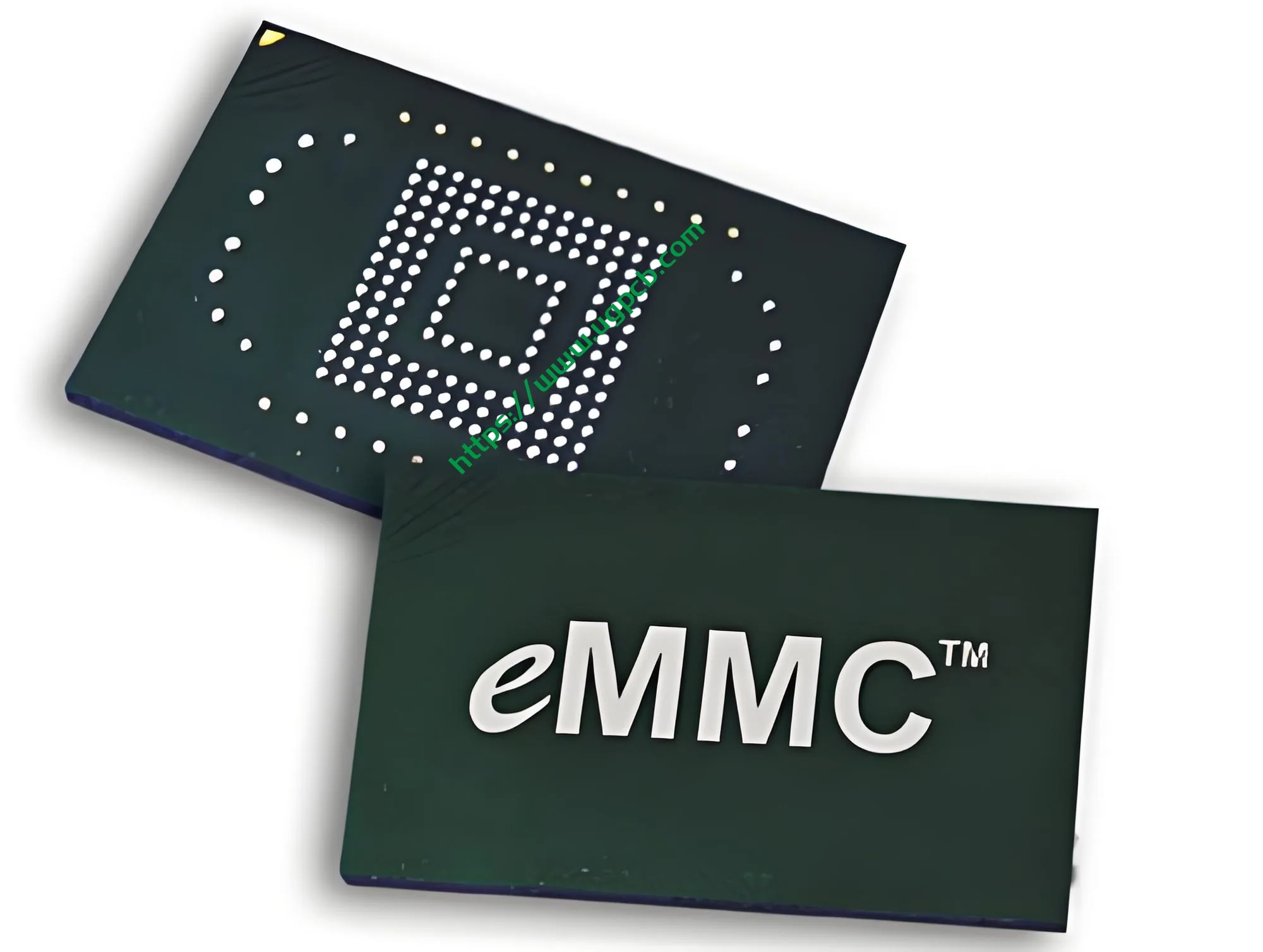
안 eMMC 패키지 기판 PCB 전문이다, 소형화된 인쇄 회로 기판 eMMC 칩 패키지 내에서 내부적으로 사용됩니다.. 코어 인터포저 역할을 합니다., 스토리지 컨트롤러 실리콘 다이 간의 전기 연결 및 물리적 지원 제공, 낸드 플래시 메모리가 죽는다, 및 외부 볼 그리드 어레이 (BGA) 인터페이스. 설계 및 제조 품질이 신호 무결성을 직접적으로 결정합니다., 열 성능, 최종 eMMC 모듈의 전반적인 신뢰성.

디자인 하이라이트 & 주요 기술 사양
고대역폭 및 소형화에 대한 eMMC 칩의 엄격한 요구 사항을 충족합니다., UGPCB의 eMMC 기판은 이러한 중요한 설계 매개변수에 중점을 둡니다.:
-
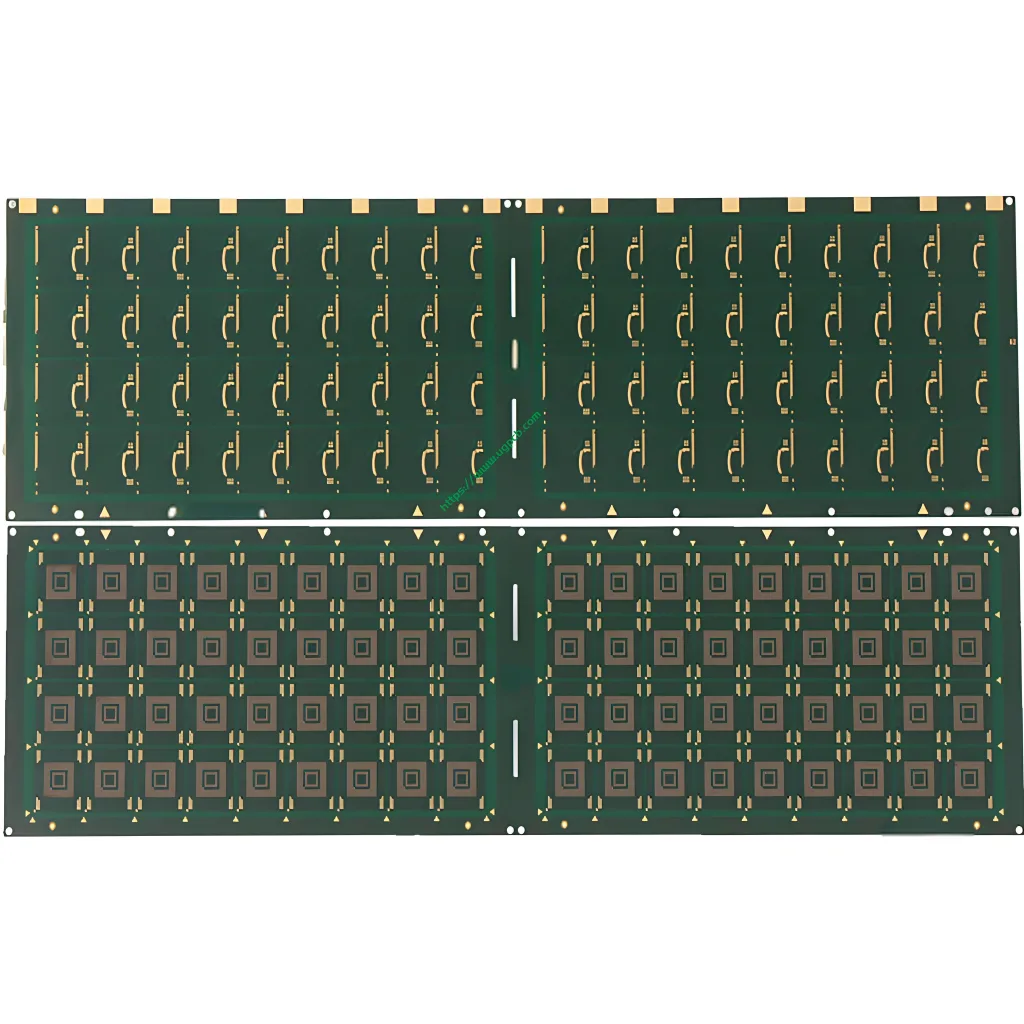
고밀도 라우팅: 초미세 회로 지원 최소 선폭/공간 20μm.
-
마이크로비아 기능: 특징 최소 비아 직경 0.1mm 고밀도 I/O 팬아웃용.
-
안정적인 적층: 4-레이어 구성 통제된 합계로 두께 0.21mm, 전기적 성능과 기계적 강도의 균형.
-
신뢰성이 높은 표면 마감: 소프트 골드 (동의하다) 도금은 산화 방지 기능을 제공합니다., 안정적인 와이어 본딩 또는 플립칩 부착을 위한 저저항 표면.
-
정밀 솔더 마스크: PSR-4000 AUS308 솔더 마스크는 우수한 절연성과 내화학성을 제공합니다..
작동 방식 & 구조적 특징
작동 방식: The substrate acts as the internal “nervous system” and “power grid” of the eMMC module. 전도성 트레이스와 마이크로 비아는 컨트롤러에서 NAND 플래시 다이로 명령 신호를 라우팅하고 데이터를 반환합니다.. 전용 전원 및 접지판으로 안정성 보장, 저잡음 전력 공급.
구조적 특징:
-
초박형 & 콤팩트: 0.21mm 최종 두께 그리고 11.5mm x 13mm 단위 크기 공간 소모 최소화.
-
고급 핵심 소재: 기반 HL832NS, 뛰어난 열 안정성과 낮은 신호 손실로 알려진 고성능 라미네이트 (낮은 Dk/Df), 열 방출에 중요한.
-
다층 아키텍처: 그만큼 4-레이어 스택업 (일반적으로 신호, 힘, 지면) 신호 경로 최적화, 누화 감소, 임피던스를 제어하고.
-
BGA 패드 어레이: 하단에는 안정적인 표면 실장 기술을 위한 정밀한 BGA 패드 레이아웃이 특징입니다. (SMT) 호스트 마더보드에 전체 모듈을 조립합니다..
기본 애플리케이션 & 사용 사례
기본 애플리케이션: 내부의 핵심 상호 연결 플랫폼 EMMC 5.1 이상 칩 패키지.
일반적인 응용 프로그램 (사용 사례):
-
스마트폰 & 정제: 기본 내부 저장소.
-
스마트 TV & 셋톱박스: 시스템 스토리지 및 캐싱.
-
IoT 장치: 스마트워치, 컴팩트한 임베디드 스토리지가 필요한 스마트 홈 허브.
-
산업 제어 시스템: 높은 데이터 신뢰성을 요구하는 임베디드 장치.
-
자동차 인포테인먼트: 자동차 등급 안정성 요구 사항을 충족하는 스토리지 모듈.


분류 & 재료 구성
-
분류: 적용등급별로 분류 가능: 소비자, 산업용, 자동차 (이 모델은 소비자를 위해 맞춤 제작되었습니다. & 고급 산업용 애플리케이션).
-
재료 쌓기:
-
코어 라미네이트: HL832NS 높은 Tg, 저손실 소재.
-
전도성 층: 고순도 전해동박.
-
솔더 마스크: PSR-4000 AUS308 (녹색, 무광택/광택 옵션).
-
표면 마감: 무전해 니켈 침지 금 (ENIG – Soft Gold).
-
성능상의 이점 & 주요 특징
-
탁월한 신호 무결성: 제어된 임피던스 및 저손실 HL832NS 소재로 안정적인 고속 데이터 전송 보장.
-
높은 신뢰성: 엄격한 공정 제어 및 재료 선택으로 장기적인 내구성 보장.
-
효과적인 열 관리: 라미네이트의 우수한 열 전도성은 활성 다이의 열 방출을 돕습니다..
-
엄격한 제조 공차: 20µm 라인/공간 및 0.1mm 마이크로 비아를 통해 입증 고급의 HDI PCB 조작 전문적 지식.
-
엔드투엔드 솔루션: UGPCB는 다음과 같은 협력 지원을 제공합니다. 기판 설계 검토 그리고 PCB 제작 에게 빠른 PCBA 프로토 타이핑.
생산 공정 개요
우리의 eMMC 패키지 기판 제조는 엄격한 기준을 따릅니다. HDI PCB 공정 흐름:
재료 준비 → 내부 레이어 이미징 → 라미네이션 → 레이저 드릴링 (0.1mm 비아) → 금속화를 통해 → 외부 레이어 이미징 (20µm 라인) → 솔더 마스크 적용 (PSR-4000) → 표면 마무리 (소프트 골드) → 전기 테스트 → 라우팅/채점 → 최종 검사 & 포장.
eMMC 패키지 기판으로 UGPCB를 선택하는 이유?
UGPCB를 선택한다는 것은 해당 분야의 전문가와 협력한다는 것을 의미합니다. 메모리 칩 기판 제조. 우리는 스토리지 인터페이스의 기술적 발전을 이해하고 귀하의 제품이 탁월한 성능을 발휘할 수 있도록 전체 체인 지원을 제공합니다., 비용, 신뢰성.
eMMC 패키지 기판 요구 사항에 대해 논의하고 견적을 요청하려면 지금 저희에게 연락하십시오.. UGPCB의 정밀 엔지니어링이 차세대 스토리지 솔루션을 위한 신뢰할 수 있는 기반이 되도록 하십시오..