
맞춤형 2레이어 리지드 FR-4 PCB: 동의하다 + Hard Gold Finish for High Reliability & 비용 효율성
Discover the industry “gold standard” for balanced performance and affordability. UGPCB’s 2-layer rigid FR-4 PCB, featuring TG150 high-temperature material and a dual ENIG + Hard Gold surface finish, delivers superior reliability for demanding applications.
나. Why Choose 2-Layer Rigid FR-4 PCB?
In the era of electronic miniaturization, 에 대한 수요 높은 신뢰성, 저렴한 비용, 그리고 compact design has made the 2-layer rigid PCB the “golden choice” for engineers and procurement managers. Unlike single-sided boards limited by routing space or expensive multi-layer boards, the 2-layer design strikes the perfect balance between performance and price.
UGPCB enhances this baseline by utilizing FR-4 TG150 heat-resistant material and a specialized 무전해 니켈 침지 금 (동의하다) + 하드 골드 표면 처리. This combination significantly improves durability and solderability, making it suitable for a wider range of harsh environments.

II. Product Core Specifications (IPC-A-600 Compliant)
The following parameters ensure full compatibility with industry standards and optimal manufacturability (DFM).
| 매개 변수 | Specification Details |
|---|---|
| 레이어 수 | 2 레이어 (양면: 맨 위 & Bottom routing, FR-4 core substrate) |
| 보드 두께 | 1.60mm (Standard industry thickness, balancing mechanical strength & 공간) |
| 기본 재료 | FR-4 TG150 (Epoxy resin glass cloth; Glass Transition Temp: 150℃; Excellent heat resistance) |
| 표면 마감 | ENIG 2u” + Hard Gold 30u” (Dual protection: Chemical immersion gold + Electroplated gold for wear resistance) |
| 구리 무게 | 1온스 (35μm) (표준 두께, sufficient for most current carrying requirements) |
| 솔더 마스크 | 녹색 (Default; 검은색, 파란색, 빨간색, White available upon request) |
| 실크 스크린 | White Epoxy Ink (Component identifiers, Logo) |
| 최소. Drill Hole | 0.3mm (12밀) |
| 최소. 선 너비/공간 | 3밀 / 3밀 |
III. 제품 정의: What is a 2-Layer Rigid PCB?
1. 정의
에이 강성 PCB is a non-flexible printed circuit board composed of a substrate, copper foil traces, 솔더 마스크, and silkscreen. It establishes fixed electrical connections through drilling and etching processes.
에이 2-레이어 리지드 PCB (Double-Sided Board) is the foundational type of rigid PCB, featuring copper traces on both the top and bottom sides of the substrate. Electrical connections between layers are achieved via Plated Through Holes (vias).
2. Classification by Layer Count
- 1-층 (Single-Sided): Circuits on one side only. Lowest cost but severe routing limitations.
- 2-레이어 (Double-Sided): Circuits on both sides. Higher routing flexibility than single-sided; moderate cost. (UGPCB’s Specialty)
- Multi-Layer (4+ 레이어): Three or more copper layers. Suitable for complex circuits but significantly higher cost.
UGPCB’s 2-layer offering represents the highest cost-performance ratio in the rigid PCB category.
IV. Design Guidelines for High Reliability
With limited routing space on 2-layer boards, 준수 IPC-2221 design standards is crucial for signal integrity and thermal management.
1. Power and Ground Layout
- 접지면: Use large copper pours for Ground (접지) to minimize signal interference and EMI.
- Power Traces: Widen VCC traces to >20밀 to reduce resistance and voltage drop.
- Spacing: Maintain a minimum 10mil clearance between power and ground to improve filtering.
2. Signal Routing
- Differential Pairs: For high-frequency signals (USB, HDMI), use differential routing to reduce electromagnetic radiation.
- 3W 규칙: Maintain a spacing of ≥3x the trace width between signal lines to avoid crosstalk.
- Return Paths: Avoid signal traces crossing splits in the ground plane to prevent signal reflection.
3. 비아 디자인
- 구멍 크기: Minimize via diameter (예를 들어, 0.3mm) to save routing space.
- Via Tenting: Use solder mask to cover vias to prevent solder paste wicking during soldering.
- 고주파: Use through-hole vias (standard for 2-layer) to minimize parasitic capacitance compared to blind/buried vias.
다섯. 작동 원리: How PCBs Work
The core function of a PCB is to connect electronic components (작은 조각, 저항기, 커패시터) via copper traces to achieve predetermined electrical functions.
- 예: In a smartphone charging board, the PCB routes power from the USB interface to the charging management chip, distributes it to the battery, and feeds battery level data back to the system via signal lines.
- While the principle is identical to 다층 보드, 2-layer boards require meticulous layout planning to ensure 신호 무결성 (그리고) within limited space.
VI. 재료 & 성능: Why FR-4 TG150?
1. 기본 재료: FR-4 TG150
FR-4 (난연제 4) is the industry standard for epoxy resin glass cloth substrates.
- High Mechanical Strength: Reinforced by glass cloth, resisting bending and breakage.
- 열 안정성: TG150 (Glass Transition Temperature 150°C) ensures stability in high-temperature environments (industrial workshops, automotive engine compartments).
- 전기적 특성: 유전 상수 (DK) 4.2-4.5, 소산 인자 (Df) 0.02, making it suitable for high-frequency signal transmission.
- 화학 저항: Resists corrosion from solder and flux, extending service life.
2. 표면 마감: ENIG 2u” + Hard Gold 30u”
Surface finish acts as the PCB’s “protective shield.” UGPCB combines two finishes for maximum benefit:
- 동의하다 (무전해 니켈 침지 금): 에이 2u” (0.05μm) gold layer deposited chemically. Offers excellent planarity and solderability, ideal for fine-pitch components (예를 들어, 0.5mm pitch chips).
- 하드 골드 (Electrolytic Gold): A thick 30u” (0.76μm) gold layer plated electrically. Provides superior wear resistance and conductivity, perfect for frequent plug-in/unplug cycles (USB ports, SD card slots).
Comparison: This combination outperforms HASL (열기 솔더 레벨링) and standard OSP (유기 용해성 보존) in high-reliability applications like 산업 제어 그리고 자동차 전자.
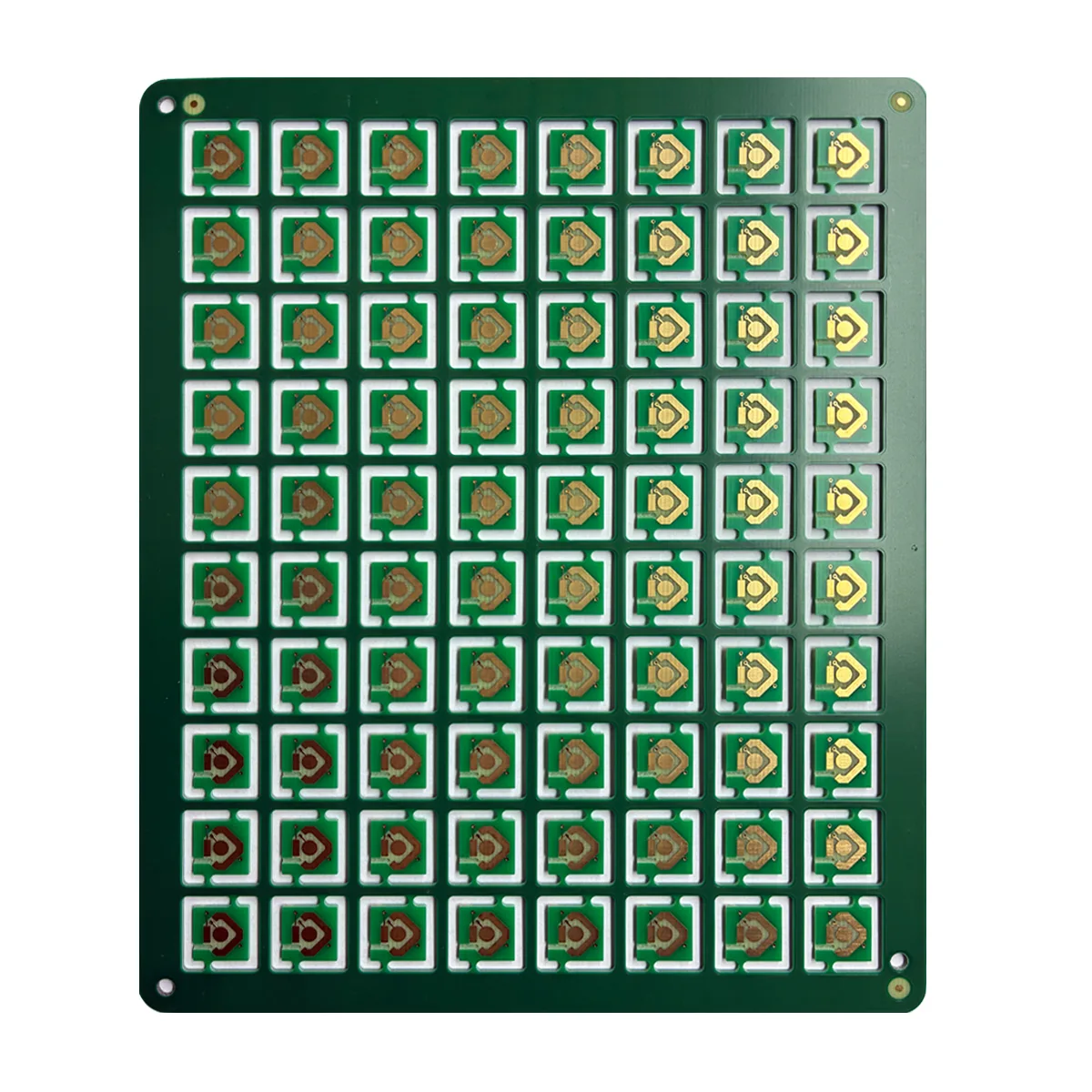
VII. 구조 & 특징: Panelization Advantages
This PCB utilizes Matrix Panelization, where multiple individual PCBs (예를 들어, 10×10 array) are arranged on a larger production panel connected by Webs (Tabs).
Advantages of Panelization:
- Production Efficiency: Multiple PCBs produced simultaneously, reducing machine setup time.
- 비용 절감: Minimizes scrap material and maximizes material utilization.
- Assembly Ease: Webs can be separated via routing or V-Cut (V-Scoring) without damaging individual boards.
Additional Product Features:
- 높은 신뢰성: FR-4 TG150 + ENIG/Hard Gold withstands harsh environments (high temp, 습기, 진동).
- 저렴한 비용: Mature 2-layer process is 30%-50% 저렴합니다 than multi-layer boards.
- 맞춤화: Supports min. 0.1mm hole size, 분. 3Mil Trace/Space, and various finishes (침수은, OSP, 등.).
- Eco-Friendly: 준수 RoHS 규제 그리고 도달하다 표준; lead-free soldering ready for global export.
VIII. 제조공정: Strict IPC-A-600 & IPC-6012 Control
UGPCB’s workflow adheres strictly to IPC-A-600 (Quality Standard) 그리고 IPC-6012 (Performance Specification for Rigid PCBs).
- 절단: Shearing FR-4 laminate to required dimensions (예를 들어, 18″x24″).
- 교련: CNC drilling for component holes (0.3mm) 그리고 vias (0.2mm).
- Electroless Copper: Chemical deposition of 1-2μm copper for interlayer connectivity.
- Image Transfer: 포토레지스트 도포, 노출, and developing to transfer circuit patterns.
- 에칭: Removing excess copper to form final traces.
- 솔더 마스크: Coating with green solder mask ink, 노출, and curing to protect circuits.
- 표면 마감: 동의하다 (2u”) + 하드 골드 (30u”) plating for solderability.
- 실크 스크린: Printing component designators (R1, C2) and logos.
- Electrical Test: 플라잉 프로브 테스트 to check continuity and isolation (no shorts/opens).
- Routing/V-Cut: Separating individual PCBs from the panel and chamfering edges.
- 최종검사: AOI (자동 광학 검사) for scratches, 산화, dimensional accuracy, and reliability tests (Thermal Shock, Vibration).
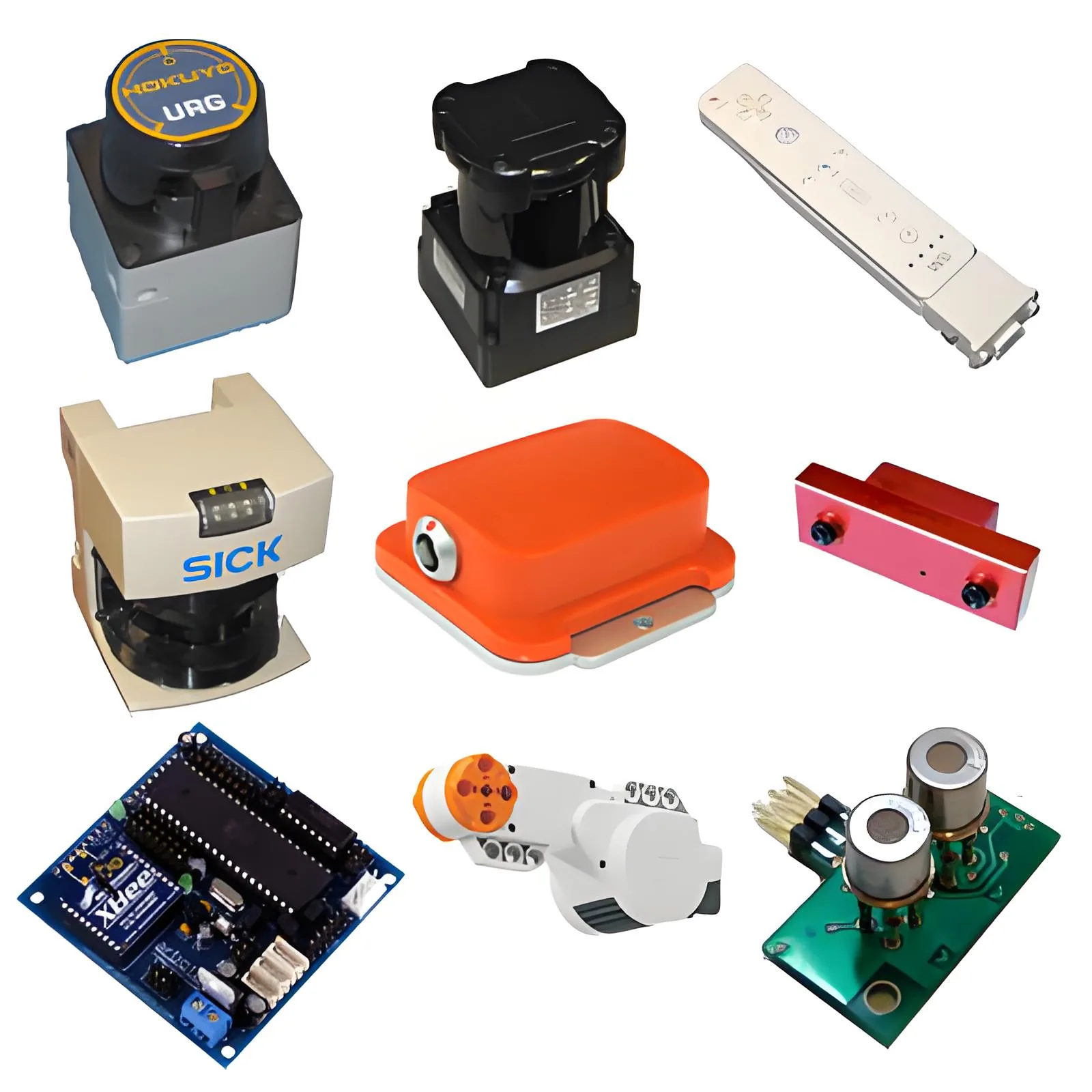
IX. 응용 시나리오
Thanks to its high reliability and cost-effectiveness, this PCB is widely used in:
- 가전제품
- Mobile/Tablets: Charging boards, 전원 모듈, keypads.
- 웨어러블: Smartwatch motherboards, fitness tracker sensors.
- Home Appliances: AC control boards, washing machine displays.
- 산업 제어
- PLC Modules: I/O boards, communication modules.
- 센서: Signal processing for temp/pressure sensors.
- 로봇 공학: Servo motor control, encoder interfaces.
- 자동차 전자
- Infotainment: Navigation mainboards, audio controls.
- 안전 시스템: Reverse radar control, TPMS (Tire Pressure Monitoring).
- EVs: Charging pile control, BMS (배터리 관리 시스템) auxiliary boards.
- 의료 기기
- Portable Diagnostics: Glucose meters, sphygmomanometers.
- Monitoring: ECG, pulse oximeter signal boards.
- Surgical: Control boards for minimally invasive instruments.
- 기타 분야
- 통신: Router/Switch interface cards.
- 항공우주: Drone flight controllers, 위성 통신.
- 스마트 홈: Smart locks, smart lighting controls.

엑스. UGPCB를 선택하는 이유는 무엇입니까??
As a professional PCB manufacturer with over 10 years of experience, UGPCB serves 1000+ clients globally.
- 고급 장비: Japanese Mitsubishi drills, German LPKF exposure machines, US Test Research flying probe testers.
- Strict Quality: 인증 ISO9001, ISO14001, and IATF16949 (자동차 산업).
- Fast Turnaround: 24-hour lead time for prototypes; 3-5 days for volume production.
- Free Services: DFM (제조 설계) Check, free quotes, and free sample testing (for first-time orders).
XI. Request a Quote: Accelerate Your Time-to-Market
If you need 2-layer rigid FR-4 PCBs or have questions about ENIG+Hard Gold 또는 panelization, contact UGPCB today!
- ✅ Free DFM Review: Optimize your design to prevent manufacturing defects.
- ✅ Free Sample Testing: Verify performance before mass production.
- ✅ 경쟁력있는 가격: Cost-effective solutions based on quantity and specs.
- ✅ 빠른 배송: Prototypes in 24h, Mass production in 3-5 날.
요약
UGPCB 2-Layer Rigid FR-4 PCB, 특징 FR-4 TG150 base material 그리고 동의하다 + Hard Gold surface finish, is the premier choice for applications demanding 높은 신뢰성 그리고 저렴한 비용. Whether you are a consumer electronics manufacturer or an automotive engineer, we provide customized solutions that meet IPC-A-600 standards.
Contact us now to start your project and seize market opportunities!