

|멀티 기가급 데이터 전송 시대에, PCB의 미크론 수준 임피던스 편차로 인해 수백만 달러 상당의 서버 어레이 성능이 저하될 수 있습니다..
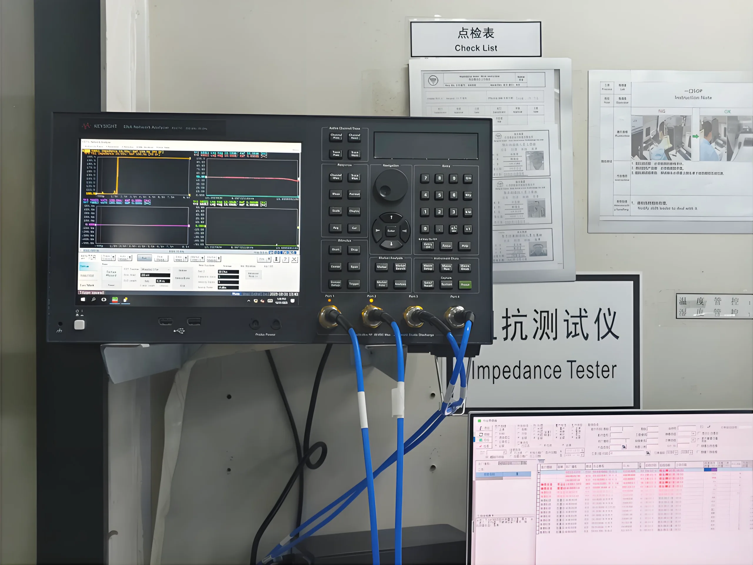
UGPCB 시설에서, 엔지니어들은 고속 서버 마더보드의 임피던스 데이터를 실시간으로 모니터링합니다.. 화면의 곡선은 녹색 통과 대역 100Ω ±2% — PCIe의 엄격한 요구 사항 5.0 차동 임피던스 표준. 이는 최첨단 기술에 대한 최신 투자로 가능해졌습니다. PCB 테스트 및 품질 관리 기술.
업계의 과제: 고속 신호 시대의 정밀 위기
AI 컴퓨팅과 5G 통신의 폭발적인 성장으로 인해 더 빠른 데이터 속도에 대한 수요가 기하급수적으로 늘어났습니다.. PCIe와 같은 표준은 다음과 같이 발전했습니다. PCIE 5.0/6.0, 신호 주파수가 다음을 초과하는 경우 32 GT/s 및 다음 방향으로 향하고 있음 64 GT/초.
주파수가 높을수록 삽입 손실이 기하급수적으로 증가합니다., 반면에 임피던스 불연속성은 PCB 흔적 신호 반사 및 지터 유발. 이러한 문제는 가장 중요한 신호 무결성 문제를 나타냅니다. 고속 PCB 설계 그리고 제조.
최신 스마트폰 마더보드에는 최소한 12 레이어 복잡한 라우팅. 소형화를 향한 끊임없는 추세는 더 좁은 트레이스 폭과 더 좁은 간격을 요구합니다., 요구사항을 추진하고 있습니다. 임피던스 제어 PCB 제조 중 전례 없는 수준으로.
기술적 솔루션: UGPCB의 키사이트 임피던스 테스트 시스템
이러한 과제를 해결하기 위해, UGPCB 통합했습니다 키사이트 4채널 20G 임피던스 테스트 시스템, 벡터 네트워크 분석기 기반의 고정밀 플랫폼 (VNA) 기술.
시스템의 핵심 활용 키사이트의 고성능 네트워크 분석기 기술, 특징 4 독립 테스트 채널 주파수 범위는 다음과 같습니다. 10 MHZ TO 20 GHz. 이 광대역을 통해 고속 상호 연결을 포괄적으로 평가할 수 있습니다., 기본 디지털 회로부터 밀리미터파 응용까지.
시스템 장점: 정밀함의 삼위일체, 능률, 안정성
-
비교할 수 없는 정밀도: 시스템은 다음과 같은 기본 임피던스 측정 정확도를 제공합니다. ±0.08% (일반적으로 ±0.045%), 임피던스 범위는 다음과 같습니다. 25 mΩ ~ 40 MΩ. 이 수준의 PCB 임피던스 테스트 정밀도는 가장 미세한 편차를 감지합니다., 이는 매우 중요합니다. 고급 PCBA 제조.
-
뛰어난 효율성: 지원합니다 다중 채널 병렬 테스트, 최대 처리량 향상 300% 단일 채널 장치와 비교. 자동화된 테스트 계획을 통해 24/7 배치 테스트 기능, 합리화 PCB 프로토타입 그리고 조립 검증 프로세스.
-
탁월한 안정성: 특징 온도 보상 기술 저팽창 재료로 제작된 광학 시스템, 시스템은 환경 변화가 측정 결과에 미치는 영향을 최소화합니다., 신뢰할 수 있는 일관된 데이터 보장 PCB 품질 보증.
애플리케이션 & 값: 프로토타입부터 생산까지 전체 주기 품질
이 고급 시스템은 UGPCB의 서비스 스펙트럼 전반에 걸쳐 가치를 제공합니다., 리더십을 강화합니다. 직업적인 PCB와 PCBA 제조 서비스.
-
R에서는&D와 프로토타이핑: 엔지니어는 다양한 스택업과 재료가 임피던스에 어떤 영향을 미치는지 신속하게 검증할 수 있습니다., 설계 테스트 주기를 몇 주에서 며칠로 단축. 이는 다음의 개발을 가속화합니다. 고주파 PCB, RF PCB, 그리고 HDI PCB.
-
대량 생산 QC 중: 스마트 생산 라인에 통합, 시스템이 샘플링 또는 전체 검사를 수행합니다., 실시간 SPC 차트 생성. 이를 통해 사전 프로세스 조정이 가능합니다., 배치 문제를 방지하고 일관된 품질을 보장합니다. 대량 PCB 생산.
-
고급 애플리케이션용: 다음과 같은 중요한 애플리케이션의 경우 AI 서버 PCB, 5G 기지국 회로 보드, 그리고 고속 스위치, UGPCB는 자세한 내용을 제공합니다. 임피던스 일관성 보고서. 이러한 데이터 투명성은 다음을 추구하는 고객과의 신뢰를 구축합니다. 신뢰할 수 있는 PCB 공급업체 그리고 턴키 PCBA 솔루션.
측정 뒤에 숨은 과학
시스템의 성능은 견고한 과학적 원리에 뿌리를 두고 있습니다.. 그것은 고용한다 시간 도메인 반사 측정 (tdr), 신호를 트레이스 아래로 보내고 반사를 분석하여 임피던스 변화와 결함을 찾아내는 방식으로 레이더처럼 작동합니다..
특성 임피던스 (z₀) 트레이스의 형상은 주로 기하학적 구조에 의해 결정되며 고주파수에서는 다음 공식으로 근사됩니다.:
Z₀ ₀ √(l/c)
(여기서 L은 단위 길이당 인덕턴스이고 C는 단위 길이당 커패시턴스입니다.). 이는 물리적 치수를 제어하는 것이 왜 중요한지 강조합니다. 제어된 임피던스 PCB 제조.
시스템은 또한 델타-L 방식, 조명기 효과를 취소하고 다중 반사를 제거하는 고급 알고리즘, 탁월한 정확도 제공 고속 및 고주파 PCB 테스트.
실질적인 고객 혜택
이 기능에 투자하면 고객에게 직접적인 이점이 제공됩니다.:
-
위험 감소: 임피던스 편차를 조기에 감지하여 비용이 많이 드는 현장 고장 및 리콜을 방지합니다..
-
향상된 성능: 정밀한 임피던스 제어로 더 높은 데이터 속도와 더 낮은 비트 오류율 가능, 이는 매우 중요합니다. 고속 디지털 PCBA 그리고 통신 장치 PCB.
-
더욱 빨라진 출시 시간: 신뢰할 수 있는 테스트 데이터로 설계 불확실성 감소, 고속 인터페이스 검증 시간 단축 40-60%.
UGPCB에, 우리의 약속은 시설 벽뿐만 아니라 우리가 배송하는 모든 보드에도 새겨져 있습니다.: “Single-Ended Impedance 50Ω ±5%, 차동 임피던스 100Ω ±8% — 30% superior to typical industry standards.” 이것은 단순한 사양이 아니다.; 고속 디지털 시대의 신호 무결성을 지키는 것이 우리의 약속입니다. 귀하의 UGPCB를 선택함으로써 PCB 제작 및 PCBA 어셈블리 필요, 가장 까다로운 설계에 필요한 정밀도를 제공할 수 있는 장비를 갖춘 제조업체와 파트너 관계를 맺으십시오..