
In the realm of analog circuit design, operational amplifiers, precision resistors, and capacitors often claim the spotlight. Yet the true determinant of system performance limits is the hidden mastermind working behind the scenes: the Printed Circuit Board (PCB). This silent foundation carries all components while governing signal integrity, noise suppression, and system reliability through every millimeter of trace, each dielectric layer, and every grounding decision.
PCB Materials Science: Decoding High-Frequency Performance Beyond FR Ratings
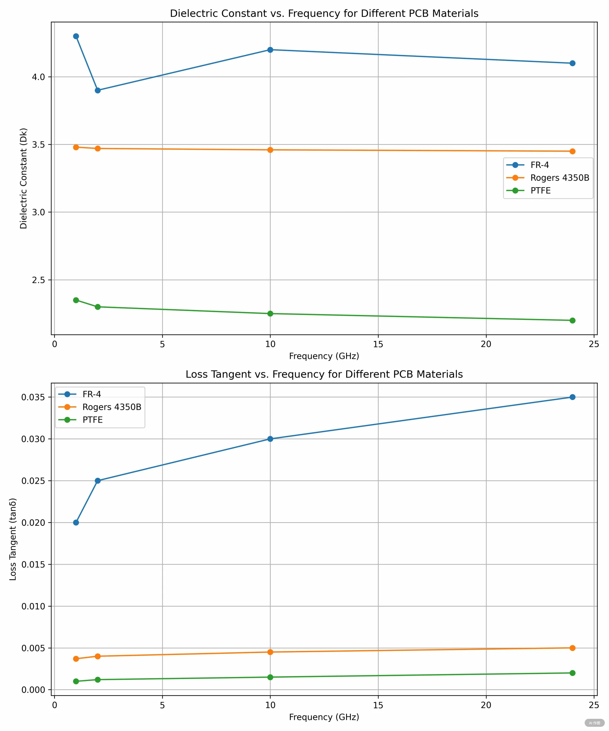
When discussing PCB materials, FR-4 flammability ratings are merely the prologue. For high-speed analog circuits, Dielectric Constant (Dk) and Dissipation Factor (tanδ) are the invisible hands shaping signal destiny.
Signal propagation velocity (v) is determined by:
v = c / √(ε_r)
Where *c* = speed of light, ε_r = relative permittivity. FR-4’s ε_r fluctuates between 4.2-4.8, causing up to 5% signal delay variation. More critically, its loss characteristics – at 10GHz, standard FR-4 exhibits tanδ=0.02, equating to 0.5dB signal loss per inch.
Humidity-Temperature Interplay proves particularly lethal in precision circuits:
-
1% moisture absorption reduces FR-4 surface resistance by three orders of magnitude
-
15% Dk drift at 85°C shifts filter center frequencies catastrophically
Expert Insight: Medical PCBs using Rogers 4350B (ε_r=3.48±0.05) maintain <2% Dk variation from -40°C to +150°C – critical for life-sustaining monitoring equipment.
PCB Stackup Architecture: Engineering Current Paths & EMI Shielding
Single/Double-Layer Limitations
Beyond 10MHz signals, 1.6mm double-sided boards reveal grounding layer weaknesses. Interlayer capacitance:
C = (ε_0 * ε_r * A) / d
Standard 1.6mm boards achieve only 35pF/in² – insufficient for >100MHz noise suppression.
Four-Layer Stackup Revolution
Dedicated power/ground planes transform impedance control:
-
0.2mm dielectrics boost capacitance to 280pF/in²
-
Ground plane resistance drops to 1/100th of single-layer
-
Radiated noise attenuation improves by 40dB
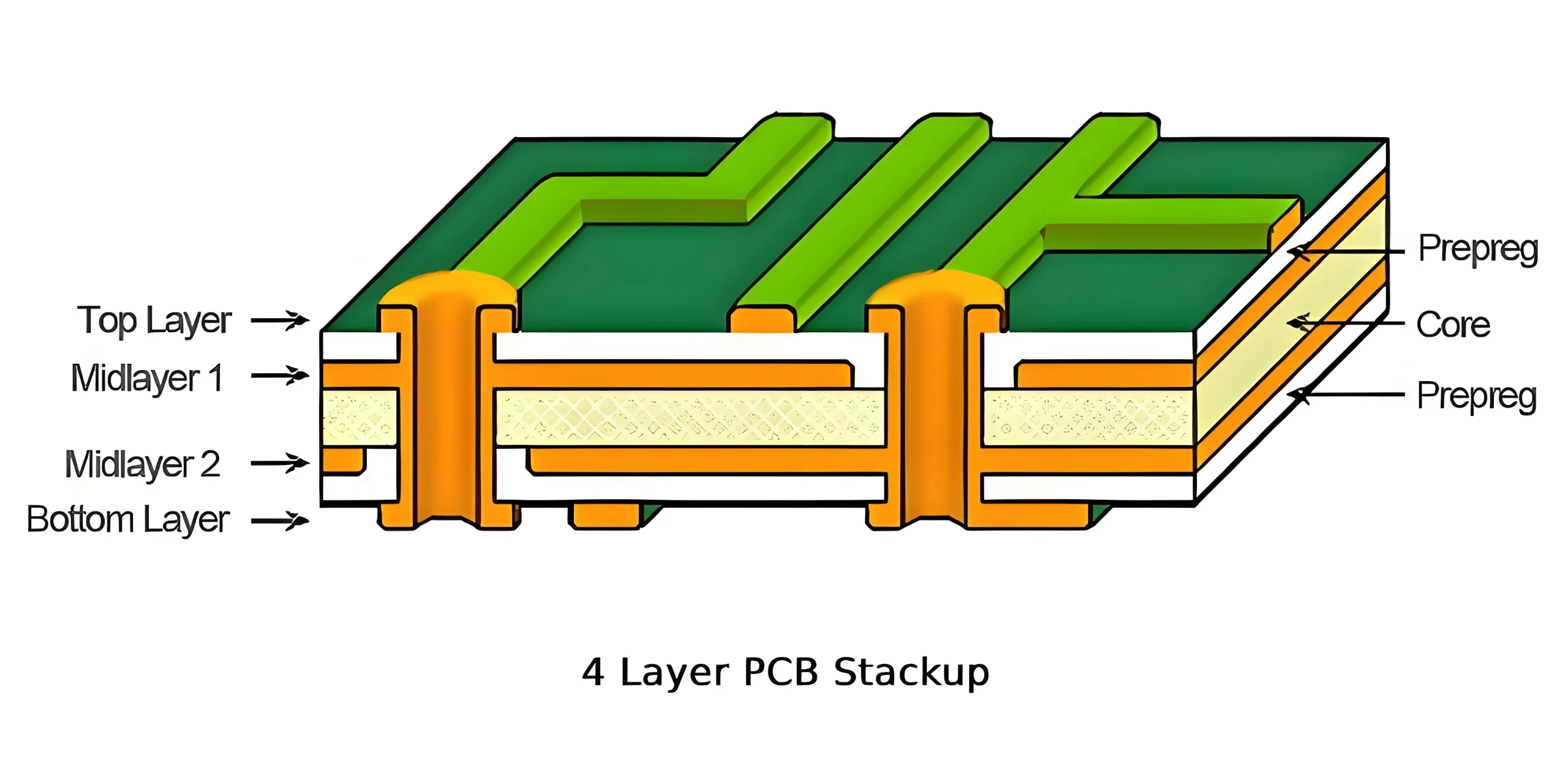 Validation Data: UGPCB lab tests show 4-layer designs reduce op-amp output noise from 78μVpp to 12μVpp – 85% improvement.
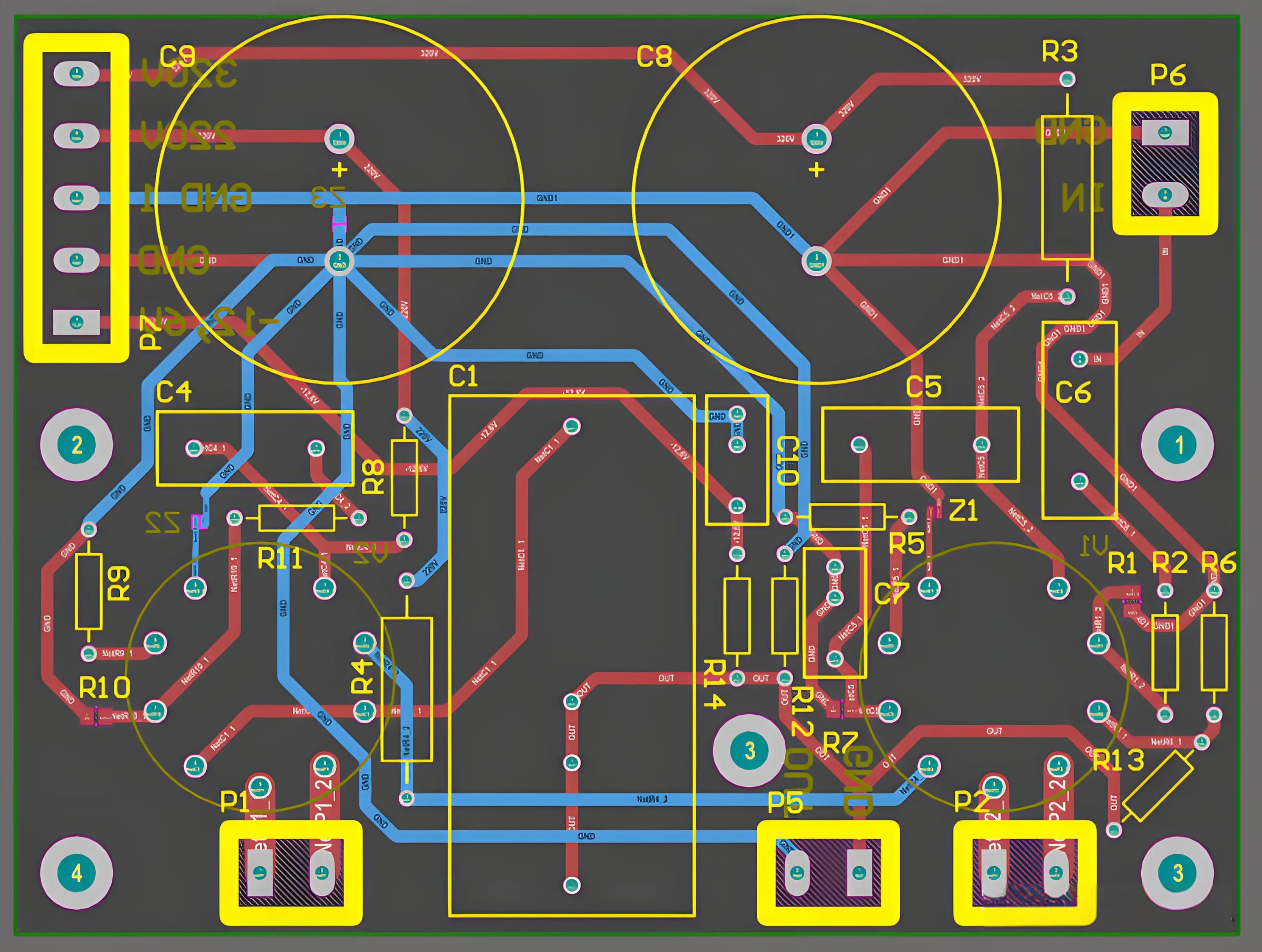
Grounding Strategies: Establishing Analog-Digital Demarcation
Plane Isolation Criticality
Overlapping digital/analog ground planes create capacitive noise channels:
C_coupling = (ε * A_overlap) / d
Even 0.1mm² overlap in 1.6mm boards generates 0.3pF coupling capacitance – enough to inject 100MHz clock noise into μV-level analog signals.
Star Grounding Principle
Single-point grounding eliminates ground loops mathematically:
V_noise = -dΦ/dt = -2πf * B * A
Where B = magnetic flux density, A = loop area. Converging paths at one point minimizes loop area.
Component Frequency Masking: When Resistors Become Inductors
Resistive Parasitics
0805 film resistors contain ≈2nH parasitic inductance. At 100MHz:
X_L = 2πfL = 1.26Ω
Exceeding typical resistance values, fundamentally altering circuit behavior.
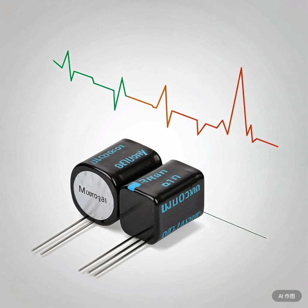
Capacitive Self-Resonance Trap
Capacitor impedance follows:
|Z| = √[R_ESR² + (X_L - X_C)²]
Standard 10μF tantalum capacitors self-resonate at 300kHz, outperformed by 0.1μF ceramics at 10MHz:
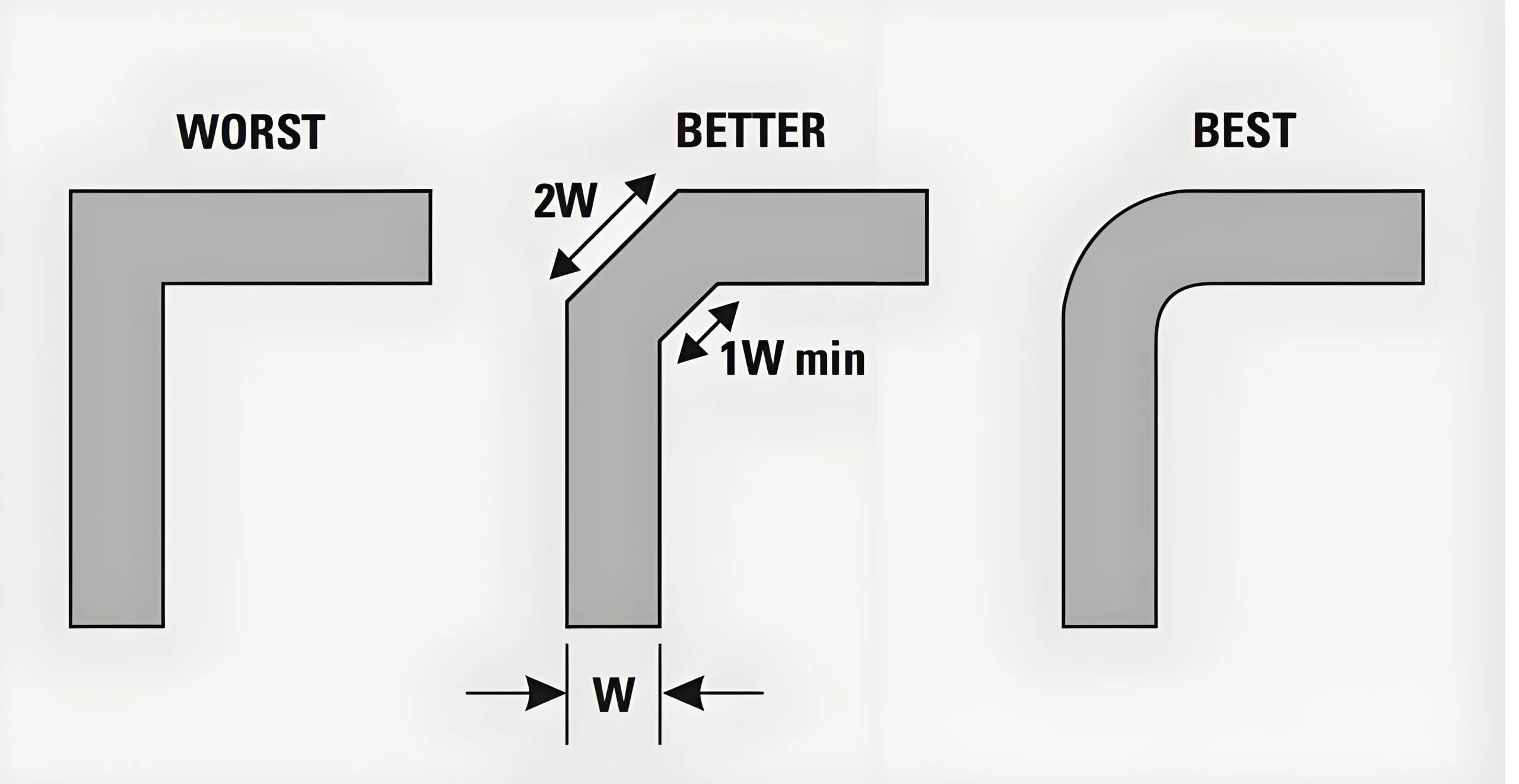
Routing Geometry: The EM Catastrophe of 90° Bend
Right-angle traces act as hidden antennas in high-speed PCB layouts:
-
Effectively increase trace length by 26%
-
Corner capacitance causes impedance discontinuities
-
Radiate 30dB more efficiently than 45° bends
Vias present equal dangers. A 0.3mm via’s parasitic inductance:
L ≈ 5.08h [ln(4h/d) + 1] (pH)
Where *h* = board thickness (mm), *d* = hole diameter (mm). At 1GHz, single via in 1.6mm board generates 1.6Ω reactance.
Ultimate Defenses: From Nano-Cleaning to Faraday Enclosures
Ionic Contamination Control
High-impedance nodes require ionic residue below:
<1.56 μg/cm² (IPC J-STD-001 Class 3)
Ultrasonic cleaning with DI water achieves <0.3μg/cm².
EMI Shielding Effectiveness
Faraday cage performance follows:
SE(dB) = 20log[(Z_0)/(4Z_s)] + 20log(e^(t/δ))
Where δ = skin depth. 1mm aluminum provides 120dB attenuation at 1GHz, but 0.1mm gaps degrade this to 30dB.
The Invisible Architect’s Revelation
Data reveals a startling truth: 68%+ circuit failures originate from PCB design flaws. Once viewed as mere component carriers, PCBs are actually mission-critical system architects.
In 10GHz circuits:
-
FR-4 dielectric loss can consume 15dB signal energy
-
0.5mm ground jumps induce 300mV ground bounce
-
Microscopic flux residues create leakage paths

The design revolution begins with paradigm shift: Reclassify PCBs from cost items to core functional elements. When laying out your next op-amp:
-
That 0.1dB noise improvement lives in laminate Dk values
-
Those 3ps timing margins reside in ground plane thickness
Elevate this “invisible architect” from backstage to center stage, and your analog circuits will shatter performance barriers.
