
In the fields of high-speed PCB design and RF circuits, impedance continuity is crucial for signal integrity. Characteristic impedance mismatch can lead to signal reflection, ringing, and distortion, severely impacting system performance. This article delves into the causes of impedance discontinuity and provides industry-proven solutions to help engineers optimize PCB designs.
Understanding Characteristic Impedance and Its Importance
Characteristic Impedance is a core concept in high-frequency PCB signal transmission. According to the IPC-2141A standard, as a signal propagates along a transmission line, an electric field is formed between the signal line and the reference plane, creating an instantaneous current. If the transmission line is uniform, an equivalent resistance is formed, defined as the ratio of voltage to current (Z=V/I). This is the Characteristic Impedance.
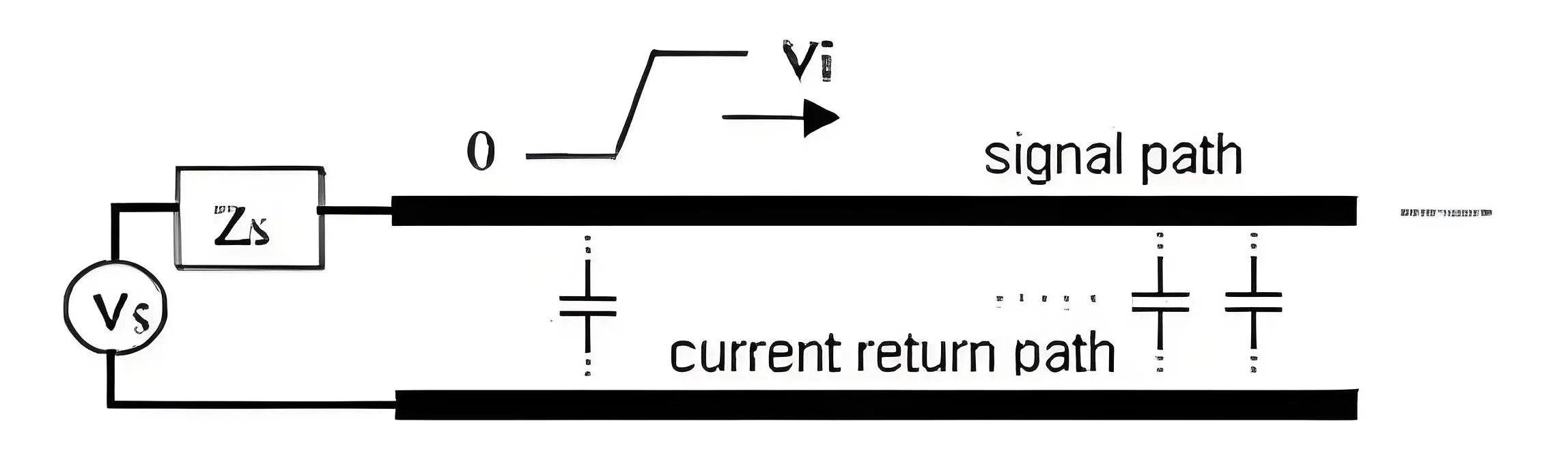
When the characteristic impedance changes along the transmission path, signal reflection occurs at the point of discontinuity. This reflection can cause signal distortion, timing errors, and electromagnetic interference (EMI) issues. According to IEEE research, an impedance deviation exceeding 10% can severely degrade signal integrity.
Key Factors Affecting Characteristic Impedance
Characteristic impedance is primarily influenced by four parameters: Dielectric Constant (Dk), substrate thickness (h), trace width (w), and copper thickness (t). The characteristic impedance formula for a microstrip line can be approximated as:
Z0 = (87 / √(εr + 1.41)) * ln(5.98h / (0.8w + t))
Where εr is the relative dielectric constant of the substrate. This formula, derived from the IPC-2141 standard, is suitable for preliminary calculations, but professional impedance calculation tools should be used for actual design.
Five Common Impedance Discontinuity Problems and Their Solutions
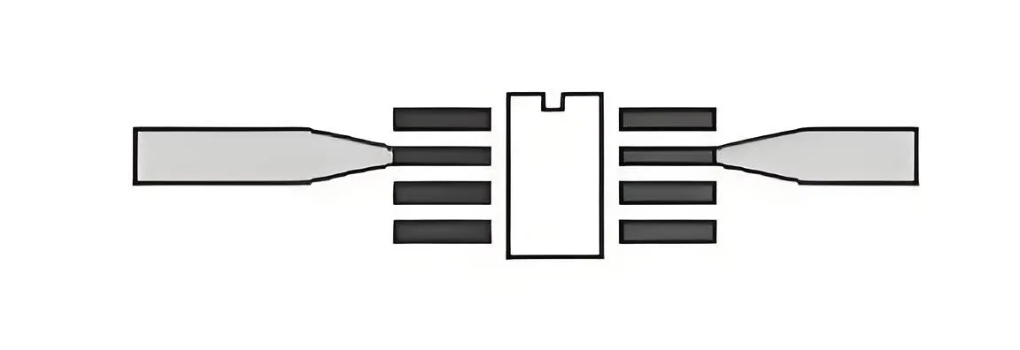
1. Sudden Trace Width Changes and Tapered Line Design
Many RF components have small package sizes, with SMD pad widths potentially as small as 12 mils, while RF signal traces often require widths above 50 mils. This size difference causes significant impedance discontinuity.
-
Solution: Use tapered lines for transitions; avoid abrupt width changes. The taper should be smooth, and its length should not be excessive. According to IPC-2221 guidelines, the taper slope should be maintained between 1:3 and 1:5 to ensure a gradual impedance change.
2. Transmission Line Corner Optimization
Right-angle bends in RF signal traces increase the effective trace width, leading to impedance discontinuity and signal reflection.
Solution: Apply miters or rounded corners. The radius of a rounded corner should satisfy R > 3W (where W is the trace width) to effectively reduce discontinuity. A 45° mitered corner is another effective method, with the miter length typically greater than 1.5 times the trace width.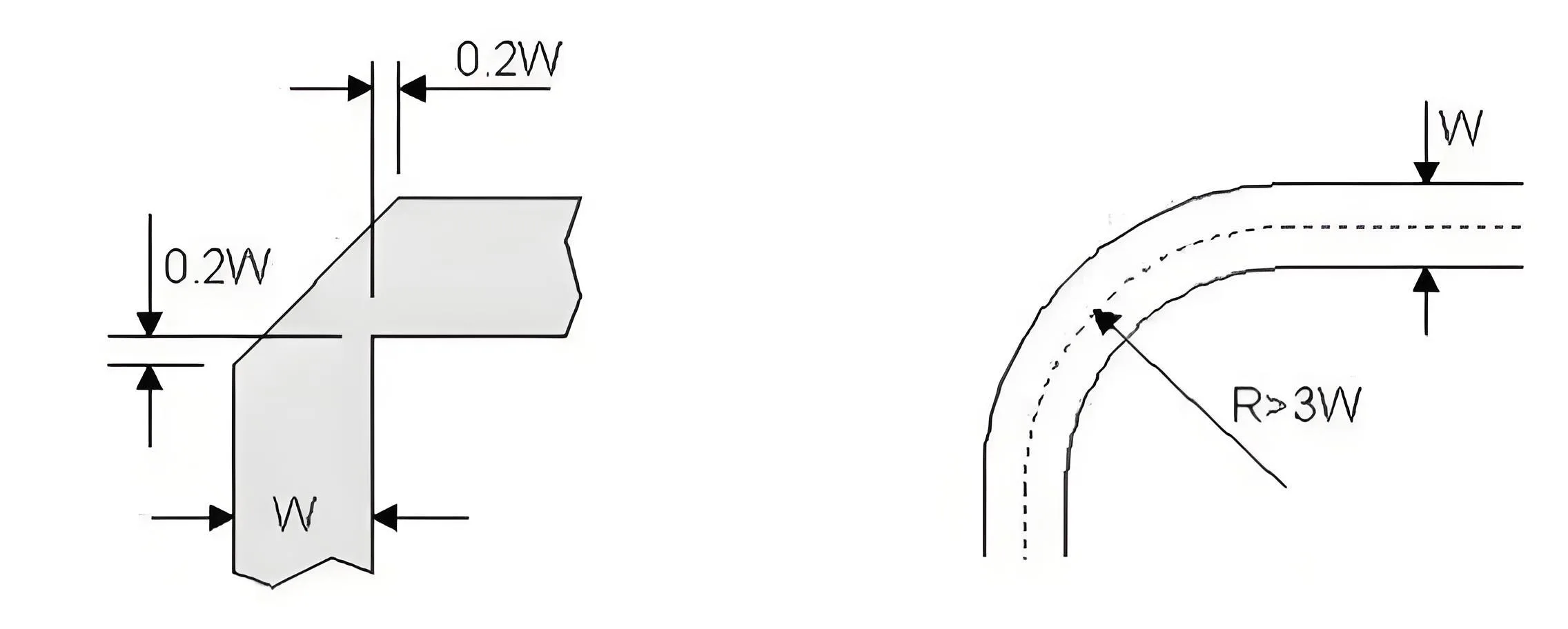
3. Mitigating the Capacitive Effect of Large Pads
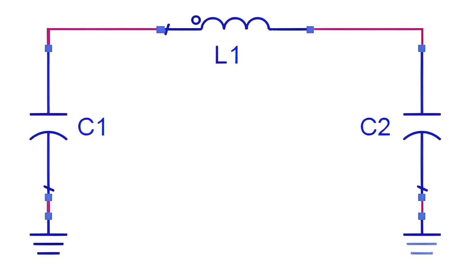
When a large component pad is placed on a 50-ohm microstrip line, it introduces parasitic capacitance, disrupting the characteristic impedance.
Solution: Combine two methods for improvement: increase the microstrip substrate thickness and create a clearance (or “cutout”) in the ground plane beneath the pad to reduce the capacitive effect. The clearance area should extend at least 20 mils beyond the pad on all sides to provide sufficient isolation.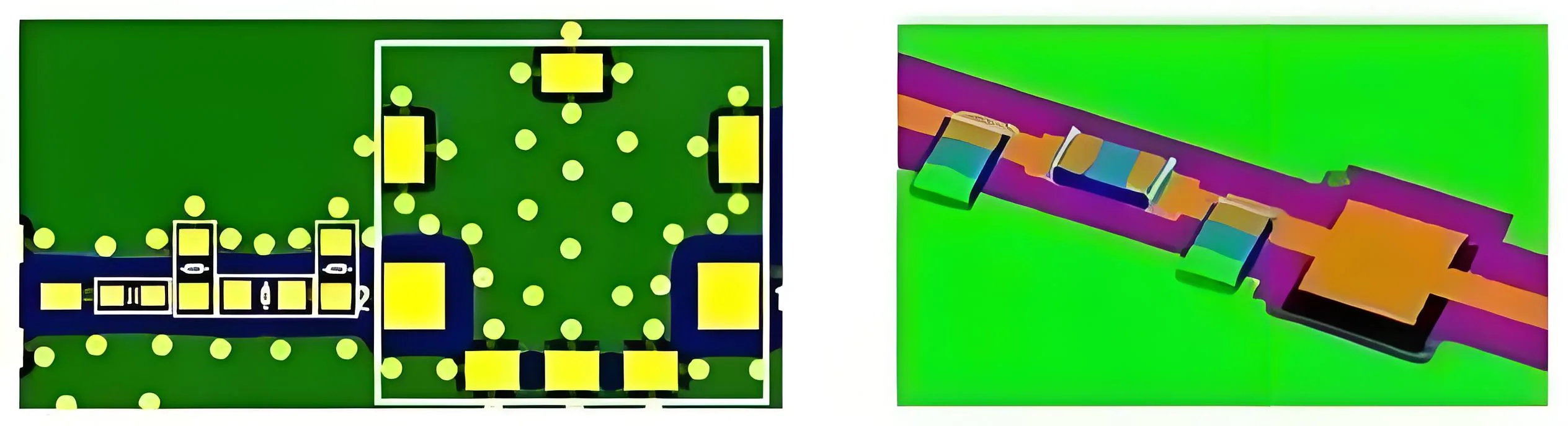
4. Optimized PCB Via Design
Vias are a primary source of impedance discontinuity due to their parasitic parameters, which affect high-speed signal transmission.
* Via Parasitic Capacitance Formula:
C = (1.41 * εr * T * D1) / (D2 – D1)
*Where T is board thickness, D1 is the via pad diameter, D2 is the anti-pad diameter, and εr is the dielectric constant.*
* Via Parasitic Inductance Formula:
L = 5.08 * h * [ln(4h / d) + 1]
Where h is the via length (stub length), and d is the drill diameter.
-
Solutions:
-
Use via-in-pad technology to minimize pad size.
-
Optimize the anti-pad diameter (typically 10-20 mils larger than the via pad).
-
Utilize back-drilling to remove the non-functional via stub.
-
For signals exceeding 1GHz, perform simulation and optimization using tools like HFSS and Optimetrics.
-
5. Thru-Hole Coaxial Connector Optimization
Thru-hole coaxial connectors present similar impedance discontinuity challenges as vias.
-
Solution: Apply the same optimization techniques used for vias, including via-in-pad, proper fanout, and anti-pad diameter optimization. Grounding vias should be placed uniformly around the connector (at least 4) to ensure excellent ground continuity.
Advanced PCB Manufacturing Technologies for Impedance Control
Modern PCB manufacturing offers enhanced capabilities for impedance control:
-
Strictly Controlled Lamination: Ensures uniform substrate thickness with tolerances within ±10%.
-
Laser Direct Imaging (LDI): Provides highly precise trace width control, with accuracy up to ±0.2 mil.
-
Surface Finish Selection: Choosing the right surface finish (e.g., ENIG, Immersion Silver) helps minimize its impact on impedance.
According to IPC-6012D, impedance control tolerance for Class 3 (high-reliability) products should be maintained within ±10%. Some demanding applications require even tighter tolerances of ±5% or stricter.
Design Verification and Testing Recommendations
To ensure impedance continuity, implement the following measures:
-
Pre-layout Simulation: Perform impedance calculations using tools like SI9000 or Polar Instruments.
-
Post-layout Simulation: Verify calculations with actual stack-up parameters.
-
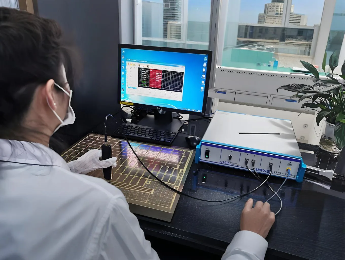
TDR Testing: Use a Time Domain Reflectometer to measure actual impedance values after production.
-
Cross-section Analysis: Periodically audit production line capabilities by checking actual dielectric thickness and trace width.
Conclusion
Impedance discontinuity in PCB design is inevitable, but its impact can be minimized through scientific design methodologies and advanced manufacturing techniques. The key to addressing this issue lies in understanding the root causes of impedance variations and applying appropriate design strategies. For high-speed and high-frequency applications, it is advisable to partner with experienced suppliers like UGPCB, which possess state-of-the-art production equipment and extensive expertise in impedance control. Such suppliers are capable of delivering PCB fabrication and PCBA assembly services that meet stringent performance requirements.
If you are looking for professional PCB manufacturing and PCBA services, contact us for an instant quote and technical support. Our engineering team will provide comprehensive impedance solutions from design to production, ensuring your product achieves optimal performance.

You actually make it seem soo eaqsy with your presentation but I
find this topic to be actually something that I think I would neverr understand.
It seems too complex and extremely broad for me.
I am looking forward for yourr next post, I will try to get the hang of it!