
The Quiet Material Revolution Reshaping Electronics
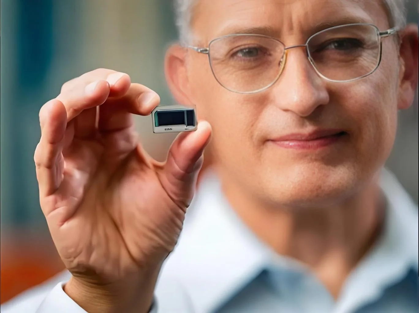
Intel’s 2024 global debut of glass substrate packaging technology detonated a seismic shift in semiconductor manufacturing. At the 2025 Suzhou TGV Industry Summit, technical leaders from Intel, TSMC, and Samsung concurred: “Glass substrates will drive semiconductor packaging into a ‘transparent era,’ with market penetration exceeding 50% within five years.” This analysis explores the technological rationale, industrial chain transformation, and implications for PCB industries.
1. Technical Superiority: Why Glass Substrates Redefine Packaging
1.1 Physical Property Dominance
Comparative analysis reveals glass substrates’ overwhelming advantages :
| Parameter | Organic Substrates | Silicon Interposers | Glass Substrates |
|---|---|---|---|
| Dielectric Constant | 4.2-4.8 | 11.9 | 3.9 |
| Loss Tangent | 0.02-0.04 | 0.001-0.01 | 0.0001-0.001 |
| CTE (ppm/°C) | 16-18 | 2.6 | 3.2-7.5 (tunable) |
| Thermal Conductivity | 0.2-0.3 | 150 | 1.1 |
| Surface Roughness | 0.5-1.0 μm | 0.05 μm | <0.01 μm |
(Source: Intel Technical White Paper, Corning Materials Lab)
Signal Loss Equation Analysis
Attenuation (α) is defined as:

With ε’≈3.9 and ε”≈0.001 for glass substrates, high-frequency (100GHz) losses reduce by 67% versus organic substrates (ε’≈4.5, ε”≈0.03).
1.2 Exponential Density Enhancement
NVIDIA’s GB200 GPU demonstrates 50%+ die count increase using glass substrates, achieving 5μm/5μm wiring density through:
-
Atomic-level flatness (<0.01μm roughness)
-
Tunable CTE matching (3ppm/°C)
-
Mechanical stability (700×700mm panel warpage <50μm)
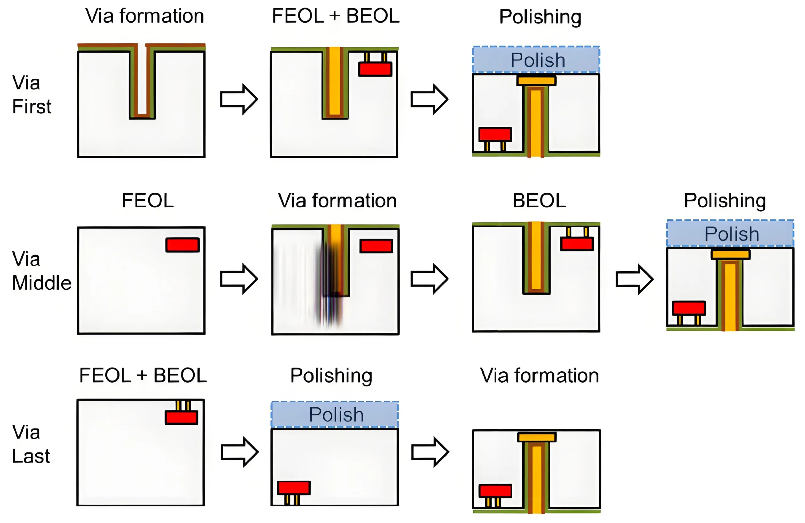
2. Process Innovations: Industrializing TGV Technology
2.1 Through-Glass-Via Manufacturing Breakthroughs
Titanrise Tech’s laser modification achieves 8,000 vias/sec at ±5μm precision (3σ), 160× faster than conventional methods. Key steps:
-
Picosecond Laser Modification: Creates micron-scale altered zones
-
HF Etching: Achieves 100:1 aspect ratio
-
Metallization: PVD sputtering + electroplating (>15MPa adhesion)
2.2 Metallization Advancements
Four technical routes address glass adhesion:
-
Electroless Cu + Micro-etching (AKM Solutions)
-
Nano-Ag Paste + LT Sintering (Wintech Patent)
-
Plasma Grafting (IME-CAS Technology)
-
PVD Ti/Cu Stack (Titanrise Standard)
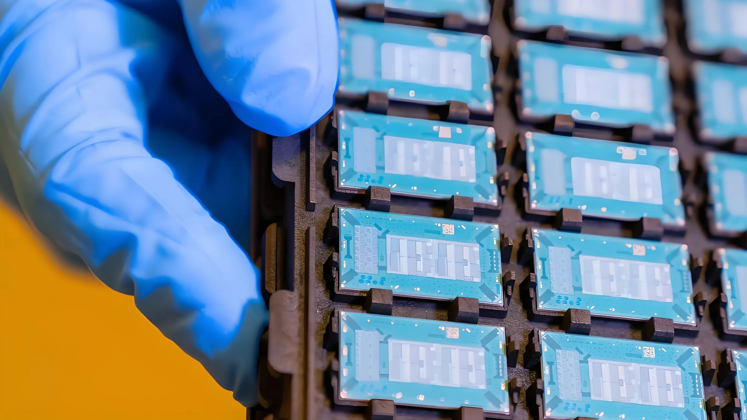
Among them, UGPCB has invested heavily in introducing the DEP600 equipment, which adopts high aspect ratio sputtering technology, achieving 95% coverage in 10:1 hole profiles, with a metal resistivity of less than 2.5 μΩ·cm, reaching an internationally leading level.
3. Industry Landscape: Global Competition Intensifies
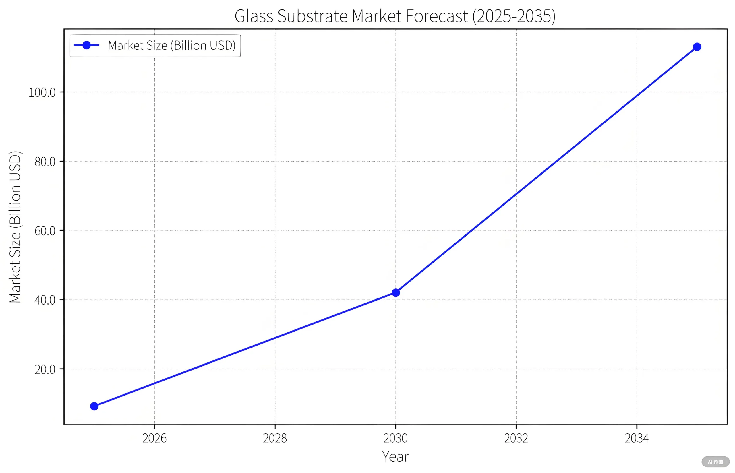
3.1 Market Growth Projections
Prismark forecasts explosive expansion:
-
2025: $916M (TGV substrates)
-
2030: $4.2B (full applications)
-
2035: $11.3B (entire ecosystem)
3.2 Geopolitical Tech Race
-
USA: Intel standards + Corning supply dominance
-
Korea: Samsung’s “Glass Alliance” + SKC’s 9-layer stacks
-
China: Wintech/AKM mass production + JFE 2026 localization
4. Challenges & Solutions: Commercialization Hurdles
4.1 Cost Reduction Pathways
Current 3-5× cost premium vs traditional substrates will plummet through:
-
85% large-panel (>2m²) utilization
-
90% laser drilling cost reduction
-
Metallization yield improvement (60%→92%)
4.2 Reliability Certification
New standards required:
-
Thermal Cycling (-55°C–250°C, 1,000 cycles)
-
EM Lifetime (MTTF >10⁷ hours @ JEP154)
-
High-Frequency Stability (<0.5dB/cm @100GHz)
5. PCB Industry Implications: Threat vs Opportunity
5.1 Market Disruption
-
30% HDI/substrate replacement risk
-
Hybrid (glass+resin) substrate opportunities
5.2 Technology Synergies
-
Picosecond laser drilling adoption
-
PVD-enhanced HDI trace precision
-
Optical inspection <0.1μm resolution
Conclusion: Transparent Substrates, Opaque Futures
China now leads critical TGV sectors (equipment, testing, materials). As Intel’s Pat Gelsinger notes: “Material innovation becomes the new Moore’s Law at atomic scales.” This glass-driven revolution may unlock semiconductor’s second growth curve.
