
In the microscopic world of printed circuit boards (PCBs), every square inch of copper foil represents a meticulously planned battlefield for engineers. When you open the “guts” of an electronic product, the shimmering metallic areas covering the blank spaces on the board are not merely decorative; they are the “invisible guardians” that determine product performance. This is PCB copper pour—the most fundamental yet often overlooked aspect of PCB design.
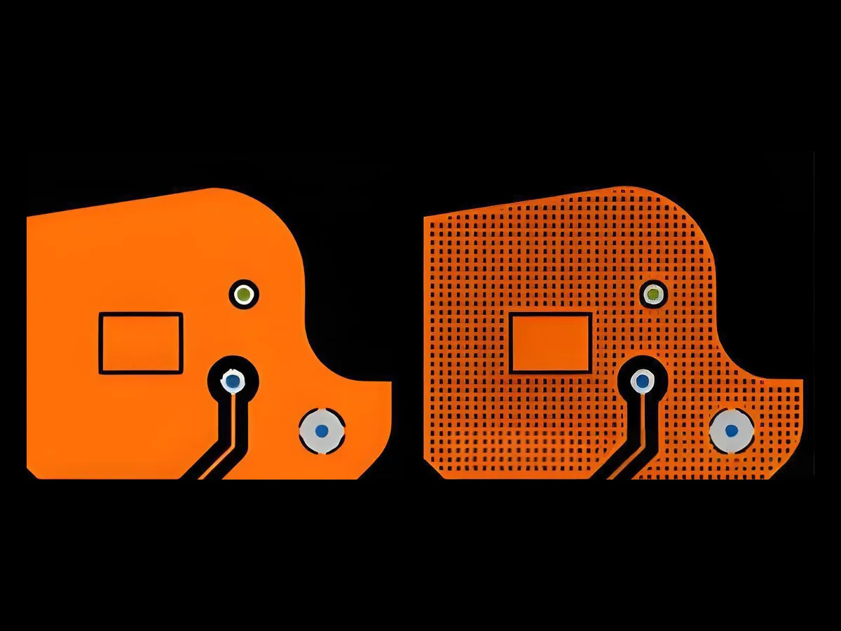
Within the realm of copper pour, two primary methodologies prevail: Solid Copper Pour and Hatched Copper Pour (also known as grid copper). They represent the “dual personality” of circuit boards: one is steady and robust, excelling at conducting current; the other is lightweight and permeable, adept at handling high frequencies. Today, we will provide an expert analysis of the essential differences between these two PCB copper pour techniques, citing authoritative data to help you make the optimal decision for your next PCB design or procurement. If you are seeking a high-precision PCB supplier, understanding these details will directly determine the success or failure of your product.
I. Electrical Performance: Low-Impedance “Highways” vs. High-Frequency “Eddy Current Killers”
From an electrical perspective, solid copper is akin to a wide, flat “highway.” It provides a continuous conductive layer. According to Ohm’s Law, its extremely low impedance ensures minimal voltage drop when carrying large currents. For low-frequency, high-current boards such as power modules or power amplifiers, solid copper pour is the undisputed champion. Furthermore, it forms a natural electromagnetic barrier, significantly enhancing the board’s Electromagnetic Compatibility (EMC).
However, in the high-frequency world, the situation reverses. While solid copper conducts electricity well, it is prone to eddy currents in changing magnetic fields. This not only causes energy loss but also interferes with signals. This is where hatched copper pour shines. Because the copper is distributed in a grid pattern, it effectively disrupts the path of eddy currents. Although its DC resistance is slightly higher than solid copper, in ultra-high-frequency circuits, its impedance can be controlled by adjusting the “window” size of the grid, sometimes offering superior shielding performance at specific frequencies .
II. Thermal Management: The Balancing Act of Heat Dissipation and Stress Relief
Heat is the enemy of electronics. In thermal management, solid and hatched copper play different roles.
The continuous layer of solid copper pour is an excellent thermal conductor, quickly spreading heat from “hotspots.” However, the flip side of this double-edged sword is that during rapid temperature changes, the significant difference in the Coefficient of Thermal Expansion (CTE) between copper and the PCB substrate (like FR-4) means large areas of solid copper increase the risk of board warping and delamination .
In contrast, hatched copper pour, with its discontinuous structure, acts like countless microscopic “expansion joints” pre-embedded in the circuit board. During reflow soldering or thermal shock, it effectively absorbs stress, significantly reducing the risk of PCB deformation. For rigid-flex or flexible PCBs (FPC) that require repeated bending, hatched copper is almost mandatory, as it grants the circuit board the necessary mechanical flexibility .
III. PCB Fabrication Process and Cost: The Economics Behind Etching Precision
From a manufacturing perspective, the choice of copper pour directly impacts product yield and cost.
The processing logic for solid copper pour is relatively straightforward. While it demands strict control over copper thickness and surface treatment, the process is mature and stable. For standard 1oz copper boards, the standard etching process is sufficient. This is why solid copper has a cost advantage and is a highly cost-effective choice .
However, manufacturing hatched copper pour is an “extreme challenge” in precision. Forming a uniform grid requires precise control over trace width and spacing. For instance, achieving a grid with 0.2mm trace width and 0.3mm spacing places high demands on the etchant’s undercut factor. According to the IPC-2221 standard, any minor etching deviation can cause drastic changes in grid impedance. This complex patterning inherently drives up PCB manufacturing costs. Therefore, unless necessary (for high-frequency or flexibility requirements), most conventional products opt for solid copper to secure a lower PCB quote .
IV. PCB Signal Integrity: The Presence and Absence of a Solid Reference Plane
This is the primary concern for digital engineers.
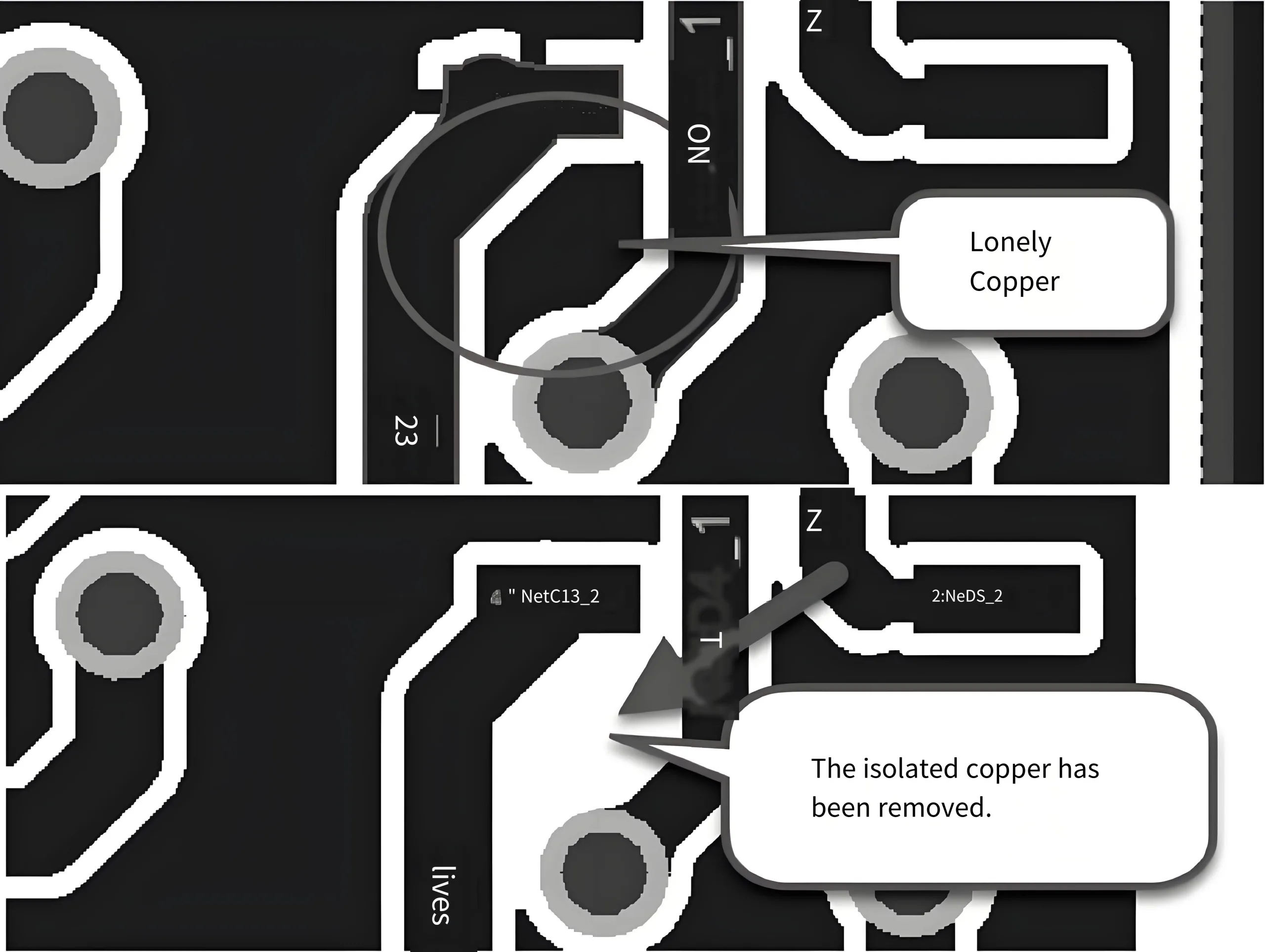
For most low-frequency and mid-frequency digital circuits, solid copper pour provides a complete return path, ensuring excellent signal integrity. Designers only need to be cautious of “dead copper” (isolated copper islands) .
However, hatched copper pour requires special vigilance regarding signal integrity. Because the grid cannot provide a solid reference plane, the characteristic impedance of high-speed signals can fluctuate when they traverse a hatched area. Research from Cadence Design Systems indicates that when routing high-speed differential pairs over hatched copper, the grid density must be strictly controlled. It may even be necessary to add coplanar ground traces on either side of the signal lines for compensation. Otherwise, signal reflection and attenuation can become “silent killers” in your design .
V. Design Decision Guide: When to Use Which Copper Pour?
To guide your design more intuitively, refer to the table below:
| Consideration | Solid Copper Pour | Hatched Copper Pour (Grid) |
|---|---|---|
| Current Carrying Capacity | Excellent. Ideal for power circuits. Per IPC-2221, for 1oz copper, a 1mm trace can carry approximately 2.3A with a 10°C temperature rise . | Fair. Current capacity is reduced due to the decreased cross-sectional area. Not suitable for high currents. |
| High-Frequency Characteristics | Excellent for low/mid-frequencies (<1GHz) . Provides good shielding. | Advantageous for high/ultra-high frequencies (>1GHz) . Reduces eddy currents and can help control specific impedance. |
| Thermal Management | Dissipates heat quickly but has high thermal stress, which can easily lead to board warping. | Thermal path is indirect, but thermal stress is low, offering strong resistance to deformation. |
| Flexible Circuits | Not suitable for dynamic bending. Can only be used in “bend-to-install” scenarios. | The only choice. The grid structure is fundamental for achieving dynamic flexure . |
| Manufacturing Cost | Low. Simple process, ideal for high-volume production. | High. Requires fine etching, longer exposure times, and generates larger data files. |
Conclusion: No Absolute King, Only the Right Choice
In the world of PCB design, solid copper and hatched copper are not mutually exclusive opposites but complementary tools. As a designer or procurement specialist, your choice should be based on the specific application of your product.
If you are designing a high-power supply or a digital system with stringent EMC requirements, solid copper pour is your go-to choice, signifying stability and low impedance. If your project involves a 5G millimeter-wave antenna or a flexible wearable device that requires repeated bending, embrace hatched copper pour; it will help you overcome the challenges of signal loss and mechanical stress.
Whichever scheme you choose, partnering with an experienced PCB manufacturer is crucial. A professional PCB supplier can not only provide an accurate quote based on your design files but also identify potential risks in your copper pour during the DFM (Design for Manufacturing) stage, ensuring your innovative concept is flawlessly realized from the drawing board to the final product. On your next design, take a few extra minutes to scrutinize your copper pour—because the devil, and the difference between success and failure, is in the details.
